[odel
339
A
Section
VIII
The
input
signal
from
input
buffer
amplifier A3U101
is
retarded
90°
by
phase shift
amplifier
A3U 1 and
applied
to the
input
of A4U4
as the
reference signal.
The output
of the
notch
amplifier (A3U3)
is
amplified by A4U 1 and
is
used by
the
phase
detector (A4U4)
as
the control
signal.
The
output
of
the
error
detector is
equal to the
product of
the
two
input
signals.
Mathematically,
the output
of
A4U4
(Vo) is
equal to
the
reference
signal [Al Cos
(wt
-
90°)]
times
the
control
signal (A2
Cos
wt
+
0)
or,
Vo
=
AlA2 [(Cos
wt
-90°)
(Cos wt +
0)].
By trig
identity, this
expression
is
equal to:
[Cos
(2
wt
+
o
-90°)
+
Cos
(o
+
90°)]
or;
Vo
=
1/2
AiA2
[sin
(2
wt
+
o)
-sin
o]
The
differential
output of
A4U4
is
converted
to
a single-
ended
output by
A4U5A
and
applied to the
integrator.
»
e
integrator
(A4U5B)
acts as a
low-pass
filter
to
the
tput signal
from the
phase
detector and responds
only
to
the
low frequency
component of
the signal. The
error
signal is,
therefore,
effectively
equal
to:
Vo
=
12
AlA2
sin
o
times a
constant "K”.
The
amplitude and phase of the
reference signal ( A
l
Cos
-
90°)
is
held
constant. Therefore,
the error
signal (Vo)
is
zero
only when
the phase
difference
between
the
reference signal
and
control signal is
equal to
90°
(Cos
90°
=
0).
Since
the
reference
signal
has purposely been
shifted
by
90°,
this
condition can
only occur when the
notch filter
is perfectly
"tuned”,
resulting
in
0°
phase shift
of the signal
through it. The
error signal from the output
of A4U5 A is
applied to
the input circuit of the integrator.
Resistors A4R48
and A4R49
determine the time constant
of
integrator A4U5B. On
the
X10
frequency range
(
10
Hz
-100
Hz)
relay A4K.1 opens to
increase the time constant.
The time
constant is increased
on this range to
prevent
distortion
which might be caused by
the phase control
t
rcuit
at low frequencies.
On frequency
ranges X100
rough X10 K.
(100
Hz
-
1 10 kHz),
relay A4K.1 is closed
to parallel
A4R49 with A4R48
to reduce the time
constant FET switch A4Q3
switches the
integrator bias
resistance to prevent offsets
at the output caused by
input
imbalance.
Amplifier
A4U5C
and diodes
A4CR13 and
A4CR14 provide a
"fast-charge” path for the
integrator
when
the notch filter is
extremely off frequency.
In this
case,
the output
of A4U5A exceeds the
break-down
voltage of A4CR13 or A4CR14
to
provide
increased
charge
current to the
integrator. As the notch filter
approaches
the proper frequency,
the output of A4U5A
no
longer exceeds the
break-down voltage of A4C R
1 3
or
A4CR14
and normal
operation resumes. The output of
integrator A4U5B is
applied to
the voltage-to-current
converter (A4U5D) and A4Q2)
which drives phase
control module A3E1.
Control module A3E1
changes the
resonant frequency of the
notch filter.
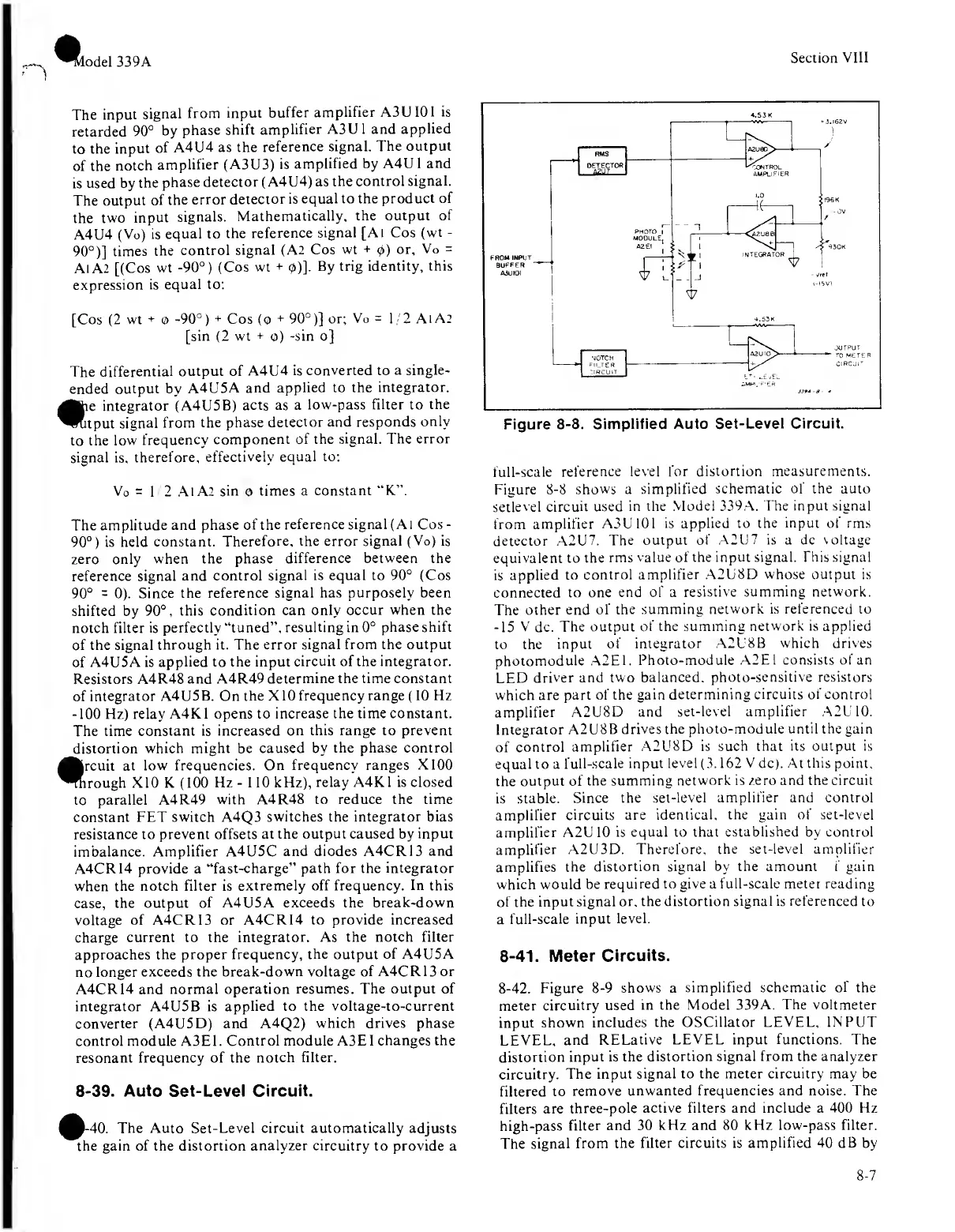
8-39.
Auto Set-Level Circuit.
P~40.
The Auto Set-Level circuit automatically adjusts
the gain of the
distortion analyzer circuitry
to
provide
a
Figure
8-8.
Simplified Auto
Set-Level Circuit.
full-scale
reference level for
distortion measurements.
Figure
8-8
shows a
simplified
schematic
of
the auto
setlevel
circuit
used in the
Model 339A. The
input signal
from
amplifier A3U101
is applied to
the input
of
rms
detector A2U7.
The output
of A2U7
is
a dc
voltage
equivalent to the
rms
value of the
input signal. This signal
is
applied
to
control
amplifier A2L8D
whose output is
connected to
one
end
of a
resistive
summing network.
The
other
end of
the summing
network is referenced to
-15
V
dc.
The output
of the summing
network is applied
to the
input
of
integrator A2U8B
which drives
photomodule A2EI.
Photo-module A2E1 consists of an
LED
driver and
two balanced,
photo-sensitive resistors
which are
part of the
gain determining
circuits of control
amplifier
A2U8D and
set-level amplifier A2U10.
Integrator
A2U8B
drives the photo-module
until
the gain
of
control
amplifier
A2U8D is such that
its output is
equal to a
full-scale
input
level
(3.
1 62
V
dc). At
this point,
the output of
the summing
network is zero and the circuit
is
stable.
Since the
set-level amplifier and control
amplifier
circuits are
identical, the gain of set-level
amplifier A2L' 10
is equal to that
established
by control
amplifier
A2U3D. Therefore,
the set-level amplifier
amplifies
the
distortion signal by the amount f gain
which
would be
required to give a full-scale meter reading
of the
input signal
or, the distortion
signal is referenced
to
a
full-scale input
level.
8-41.
Meter
Circuits.
8-42.
Figure
8-9
shows
a
simplified
schematic of
the
meter
circuitry used
in the
Model 339A. The voltmeter
input
shown includes
the OSCillator
LEVEL,
INPUT
LEVEL,
and
RELative
LEVEL
input
functions.
The
distortion
input is the
distortion signal from the analyzer
circuitry.
The
input signal to the meter circuitry may be
filtered to
remove
unwanted frequencies and noise. The
filters are
three-pole
active filters and include a
400
Hz
high-pass
filter and 30
kHz and 80 kHz low-pass filter.
The signal
from
the filter circuits is
amplified 40 dB
by
 Loading...