I'
•
.
~;.
,I
" }
, ,
')
I
, 'I:
'\""
"" y
, .
1 i It,
'r
.
I.,
.
t',·
\)
, ,
! I' • '
"
"
J\,Jod~l.
8730A'&
"B
Series
"
" '
•
I',
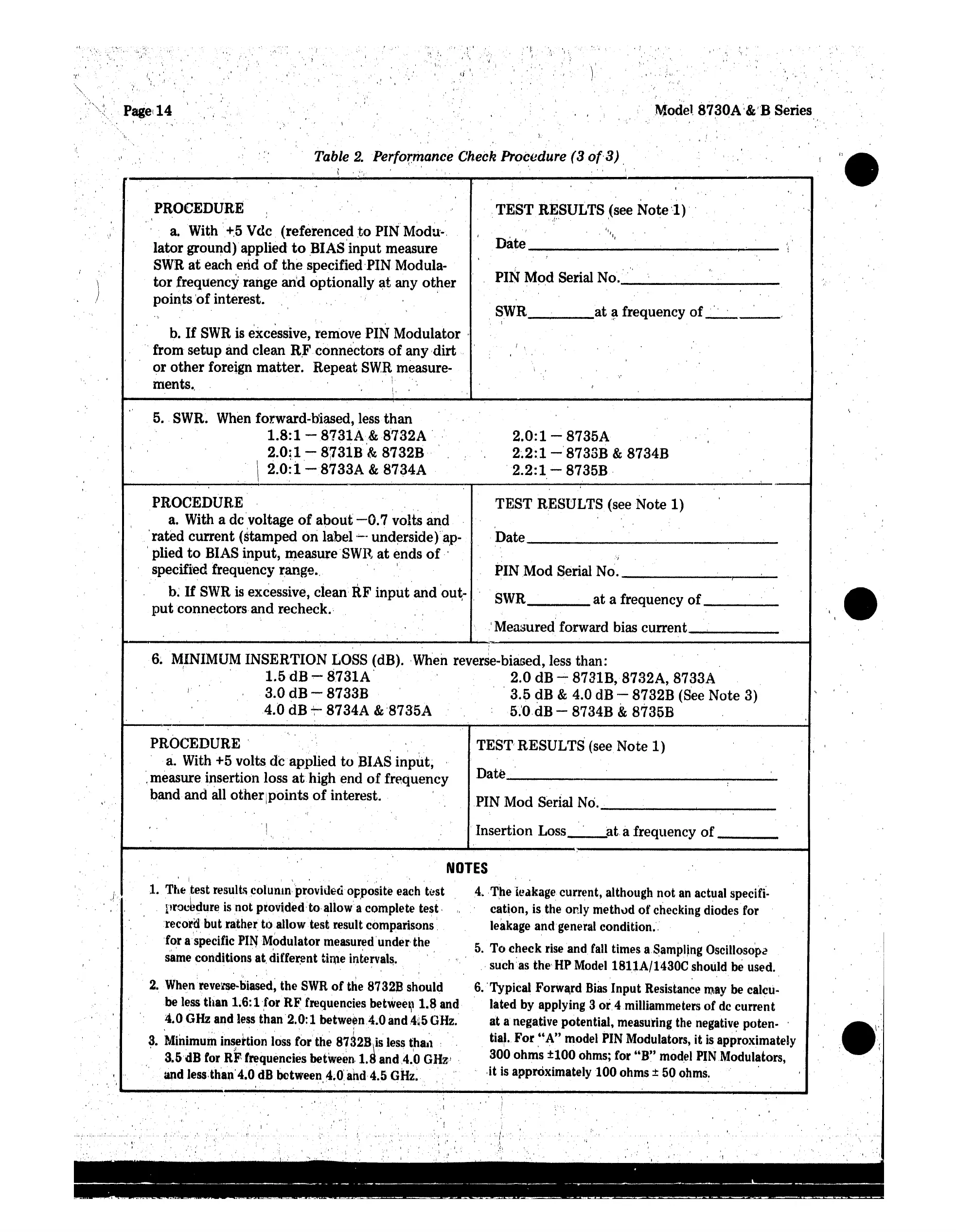
Table 2.PerfofrY1:ance Check Procedure
(3
o(3)
,
"
','
I \
PIN M()d Serial No._·
__
.........
_
TEST
R~SULTS
(see
Note
'1) ,
. "
"
, 'I,
Date
......-
__
'(
SWR
ata
frequency of..;...._.
__
I
,PROCEDURE :
a.With
+,5
Vdc (referenced
to
PIN Modu-
lator ground)'applied
to
BIAS input measure
SWR
at
each end
of
the
specifiedPlbl Modula-
tor
frequency range
and
optionally
at
any
other
points 'of interest.
b.
If
SWRis excessive, remove PIN
Modulator,
,from setup and clean R,Fconne'ctors
of
any.dirt
or
other
foreign
matter.
Repeat SWR measure-
. ,
ments, 'I,
,
)
5. ,SWR. When forward-biased, less
than
1.8:1-8731A&8732A'
2.0~1
-
8~3iB
'&
8732B '
\
2.0:i.-8733A
& 8734A
2.0:1 -
8735A
2~2:1
.:
8733B & 8734B
, 2.2:1 - 8735B .
PROCEDURE
"TEST
RESTILTS (see Note 1)
a. With a de'voltage
of
about
-0.7
volts and
'rated current (stamped
on
label·--·
undersidejap-
,Date
....;....
_____
,plied
to
BIAS input,
measureSwlt
at
ends
of
'
')
specified frequency range. ' PIN Mod Serial
NO.
.r---
_
b.
If
SWR is excessive, clean' RF
input
and out- SWR
at
a frequency
of
_
put
connectors and
recheck.
, '
I'" .Measured forward bias
current_~
_
,
6. MINIMUM INSERTION LOSS (dB).
,When
reverse-biased, less than:
I ,
1.5
dB -
8731A'
,
2.0
dB - 8731B, 8732A, 8733A
I
,3.0
dB - 8733B
3.5
dB & 4.0 dB - 8732B (See Note 3)
4.0 dB 7- 8734A &'8735A 5.'0
aa
- 8734B s 8735B
" ,
PROCEDURE
a. With +5 volts.
de applied
to
BIAS
input,
"measure insertion loss
at
high end
of
frequency
band and all
otherjpointsof
interest.
TEST'RESULTS (see Note 1)
Date --:-
__
.PIN Mod Serial No..
-------'-~---
'1
"Insertion Loss at,afrequency
of
_
NOTES
, I
A.
\',.'
:.'
,4.
,The leakage current, although not an actual speclfl-
cation, is the only method
of
checking diodes for
leakage and general condition",
5.
To check riseandfaU times aSamplJng Osclllosope
.'
suchas
theHf'
Modell8llA/1430C
should be used.
6.:Typical Forward
Bias
Input Resistance
may
be calcu-
lated by applying 3 or,4milliammeters of dc current
at a negative potential,
measuring the negative poten-
tia~.
For
,"A" model PIN Modulators, it is approximately
300 ohms
±lOO
ohms; for
"B"
model PIN Modulators,
,it is approximately
100
ohms ± 50
ohms,
1. The test resultscolumn-provided opposite each test
.
proc~~ure
is not provided
'to
allow acomplete
test
"
, . , '
'.
I
record but rather
toallowtest
result comparisons.
'for aspeelftc
PIl\JM~dulator
measuredunder' the
same conditions at,
diffe~nt
time
tntervals,
. ,
"
2
..
WhenrevelSe-biased~
the
SWR
of
the
873213
should
be less than
1~6:
i',eor
R~
frequencies
betwee~l
1.~
and
4.0 GHz and less than 2.0:1
betwe~n4.0
and
4~5
GHz.
,
" . ,
.'
I,
"
3. Minimum
in~l1ion
loss.for
lh~
8732B\is less than • '.
., 3.5 dB for
RF;
frequenCies between-l.8 and ,4.0
GHz,
I .
and less·tban'4.0 d:Bbctween,4.0'ahd4.5
GHz~
,,"
,
L-
.....
__
~
......
..;..._~
~-'-----~-----------~
......
,I
, " I
I'
I"
.,
• f
I,
~.
,
\
"I
-,
. I
I'
.
'\
.
~
...
__
._.
~___
_ ,....--
--L-.-
_
.
..
----
--
--
._
..
_.
- ---
---
-------,-----........------..
----------
 Loading...