LOCAL
BUS
INTERFACE
The analyses that follow are based
on
the assumption that a 16-MHz 80386
is
used.
If
the
processor
is
operated at a different frequency, the timings will change accordingly. Example
worst-case signal parameter values from the
80386 Data Sheet (Order Number 231630) are
used; consult the most recent data sheet to confirm these values. Also note that delay times
and setup times must be factored into the timing of system response and interaction with
the
80386 to ensure comfortable margins for all critical timings.
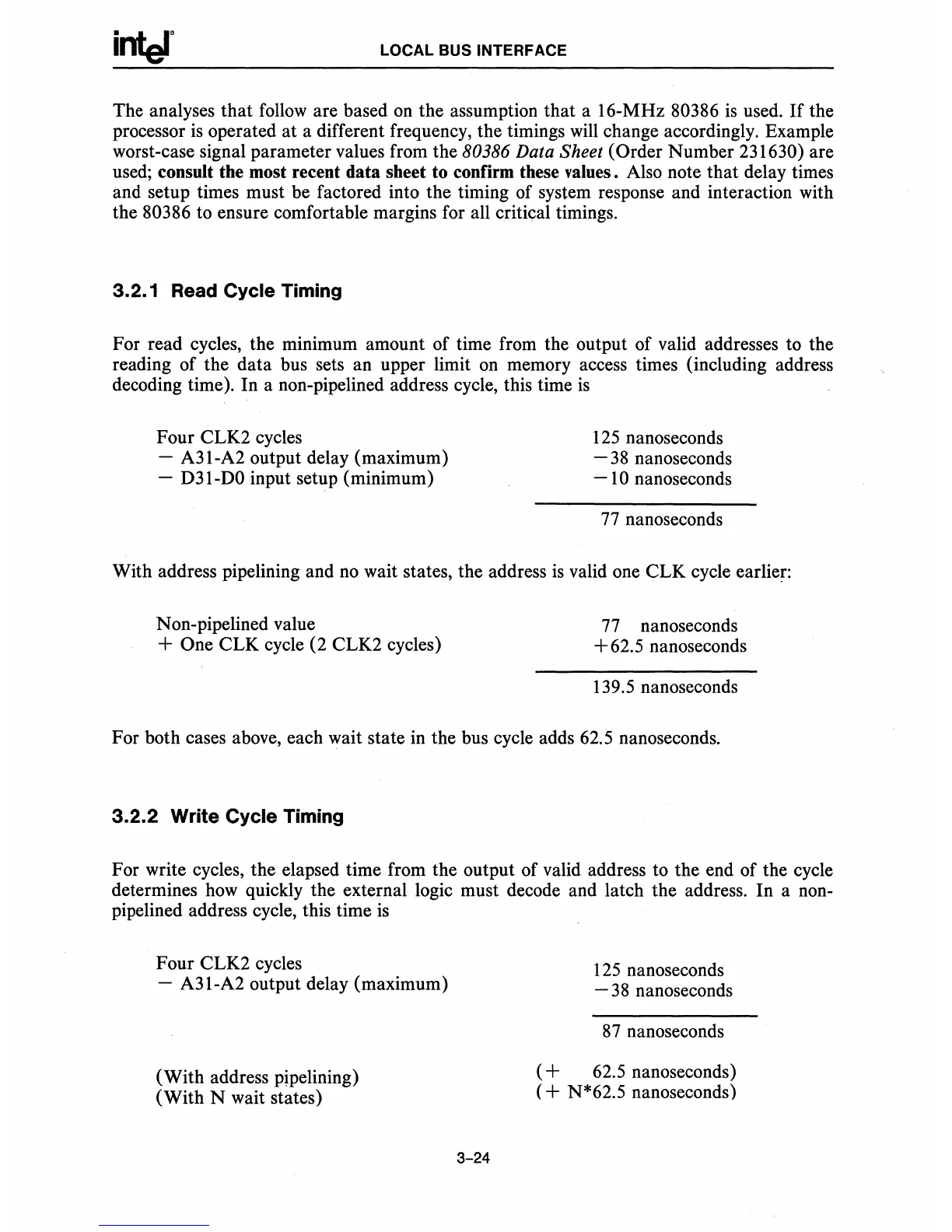
3.2.1 Read Cycle Timing
For read cycles, the minimum amount of time from the output of valid addresses to the
reading of the data bus sets an upper limit
on
memory access times (including address
decoding time). In a non-pipelined address cycle, this time
is
Four CLK2 cycles
- A31-A2 output delay (maximum)
-
D31-DO
input setup (minimum)
125
nanoseconds
-
38
nanoseconds
-
10
nanoseconds
77
nanoseconds
With address pipelining and
no
wait states, the address
is
valid one CLK cycle earlier:
Non-pipelined value
+ One CLK cycle (2 CLK2 cycles)
77
nanoseconds
+
62.5
nanoseconds
139.5 nanoseconds
For both cases above, each wait state
in
the bus cycle adds 62.5 nanoseconds.
3.2.2
Write Cycle Timing
For write cycles, the elapsed time from the output of valid address to the end of the cycle
determines how quickly the external logic must decode and latch the address. In a non-
pipelined address cycle, this time
is
Four CLK2 cycles
- A31-A2 output delay (maximum)
(With address pipelining)
(With N wait states)
3-24
125
nanoseconds
-
38
nanoseconds
87
nanoseconds
(+
62.5 nanoseconds)
(+
N*62.5 nanoseconds)