EasyManua.ls Logo

JVC GR-D350UC

JVC GR-D350UC
26 pages
To Next Page IconTo Next Page
Loading...
COPYRIGHT © 2006 Victor Company of Japan, Limited
No.YF123SCH
2006/1
DIGITAL VIDEO CAMERA
SCHEMATIC DIAGRAMS
CD-ROM No.SML200601
GR-D350UC, GR-D350US
Lead free solder used in the board (material : Sn-Ag-Cu, melting point : 219 Centigrade)
For disassembling and assembling of MECHANISM ASSEMBLY, refer to the SERVICE MANUAL No.YF081(MECHANISM ASSEMBLY).
GR-D350UCM, GR-D350USM[M6D1S3]

Other manuals for JVC GR-D350UC

Question and Answer IconNeed help?

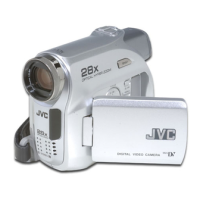
Do you have a question about the JVC GR-D350UC and is the answer not in the manual?

JVC GR-D350UC Specifications

General IconGeneral
BrandJVC
ModelGR-D350UC
CategoryCamcorder
LanguageEnglish

Summary

CHARTS AND DIAGRAMS

Schematic Diagram Interpretation

Guidelines for understanding schematic symbols, component values, and voltage readings.

Circuit Board Design Notes

Information on component/foil sides and part location guides for circuit boards.

BOARD INTERCONNECTION

MAIN(MAIN IF) SCHEMATIC DIAGRAM

MAIN(CPU) SCHEMATIC DIAGRAM

MAIN(MDA) SCHEMATIC DIAGRAM

MAIN(AUDIO) SCHEMATIC DIAGRAM

MAIN(PARAGON) SCHEMATIC DIAGRAM

MAIN(VIDEO) SCHEMATIC DIAGRAM

MAIN(PREREC) SCHEMATIC DIAGRAM

MAIN(CDSTG) SCHEMATIC DIAGRAM

MAIN(OP DRV) SCHEMATIC DIAGRAM

MAIN(REG) SCHEMATIC DIAGRAM

MAIN(MONIVF) SCHEMATIC DIAGRAM

MAIN(JACK) SCHEMATIC DIAGRAM

CCD SCHEMATIC DIAGRAM

CCD Sensor Connections

Details the connections and interface for the CCD image sensor.

REAR SCHEMATIC DIAGRAM

Rear Panel Interfaces

Details connections for battery, AV jack, and various switches.

OPE, ZOOM UNIT SCHEMATIC DIAGRAM

OPE and Zoom Unit Controls

Details control signals for the optical pickup and zoom mechanism.

VF SCHEMATIC DIAGRAM

MONITOR SCHEMATIC DIAGRAM

MAIN CIRCUIT BOARD LAYOUT (FOIL SIDE)

MAIN CIRCUIT BOARD LAYOUT (COMPONENT SIDE)

CIRCUIT BOARD LAYOUTS (CCD, REAR, OPE)

CCD Circuit Board Layout

Component placement diagram for the CCD circuit board.

REAR Circuit Board Layout

Component placement diagram for the REAR circuit board.

CIRCUIT BOARD LAYOUTS (MONITOR, VF)

Monitor Circuit Board Layout

Component placement diagram for the Monitor circuit board.

VF Circuit Board Layout

Component placement diagram for the VF circuit board.

VOLTAGE CHARTS

Voltage Measurement Data Reference

Specific voltage readings for ICs in REC and PLAY modes for calibration.

POWER SYSTEM BLOCK DIAGRAM

Power Supply Flow

Diagram showing power routing to major system blocks.

VIDEO SYSTEM BLOCK DIAGRAM

Video Signal Path Overview

Traces video signals through processing stages to display.

Related product manuals