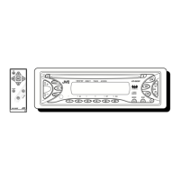
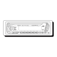
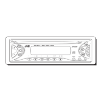
KD-S595
(No.49768)1-29
• Pin function
Pin No. Symbol I/O Function
1 PD I APC amp input terminal
2 LD O APC amp output terminal
3 LD ON I APC ON/OFF control terminal
4 LDP - Connect to ground
5 VCC - Power supply
6 RF- I Inverse input pin for RF amp
7 RF OUT O RFamp output
8 RF IN I RF input
9 C.AGC I/O Connecting pin of AGC loop filter
10 ARF O RF output
11 C.ENV I/O A capacitor is connected to this terminal to detect the envelope of RF signal
12 C.EA I/O A capacitor is connected to this terminal to detect the envelope of RF signal
13 CS BDO I/O A capacitor is connected to detect the lower envelope of RF signal
14 BDO O BDO output pin
15 CS BRT I/O A capacitor is connected to detect the lower envelope of RF signal
16 OFTR O Of-track status signal output
17 /NRFDET O RF detection signal output
18 GND - Ground
19 ENV O Envelope output
20 VREF O Reference voltage output
21 LD OFF - Connect to ground
22 VDET O Vibration detection signal output
23 TE BPF I Input pin of tracking error through BPF
24 CROSS O Tracking error cross output
25 TE OUT O Tracking error signal output
26 TE- I Inverse input pin for tracking error amp
27 FE OUT O Output pin of focus error
28 FE- I Inverse input pin for focus error amp
29 FBAL I Focus balance control
30 TBAL I Tracking balance control
31 PDFR I/O F I-V amp gain control
32 PDER I/O E I-V amp gain control
33 PDF I I-V amp input
34 PDE I I-V amp input
35 PD BD I I-V amp input
36 PD AC I I-V amp input
w
w
w
.
x
i
a
o
y
u
1
6
3
.
c
o
m
Q
Q
3
7
6
3
1
5
1
5
0
9
9
2
8
9
4
2
9
8
T
E
L
1
3
9
4
2
2
9
6
5
1
3
9
9
2
8
9
4
2
9
8
0
5
1
5
1
3
6
7
3
Q
Q
TEL 13942296513 QQ 376315150 892498299
TEL 13942296513 QQ 376315150 892498299
http://www.xiaoyu163.com
http://www.xiaoyu163.com
 Loading...