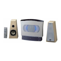
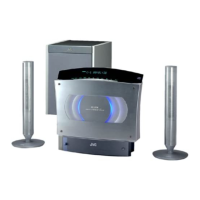
VS-DT2000
1-29
41
42
43
44
45
46
47
48
49
50
51
52
53
54
55
56
57
58
59
60
61
62
63
64
X1
VSS1
FLAG
BLKCK
/RFDET
EQx2
EQx4
P71/TIO1
FWD
REW
IREFx4
P75/BUZ
/RESET
STAT
/DMUTE
/P.ON
MLD
MDATA
MCLK
P43/AD3
P44/AD4
P45/AD5
/SW2
/SW3
-
-
I
I
I
I
I
-
O
O
O
-
O
I
O
O
O
O
O
-
-
-
I
I
Connect to external crystal oscillator
Ground terminal
Flag signal input
Sub code block clock signal input
RF signal amplitude detecting signal input
Equalizer select signal input
Equalizer select signal input
Not use
Loading (EJECT) output
Loading (LOAD) output
Switching signal for IREF current (4x mode : L)
Not use
Reset signal output (L: reset)
Status signal input
Muting output
Power ON/OFF switching signal output
Microcomputer command load signal output
Microcomputer command data output
Microcomputer command clock signal output
Not use
Not use
Not use
Mechanism switch (Loading switch)
Mechanism switch (Chucking completion)
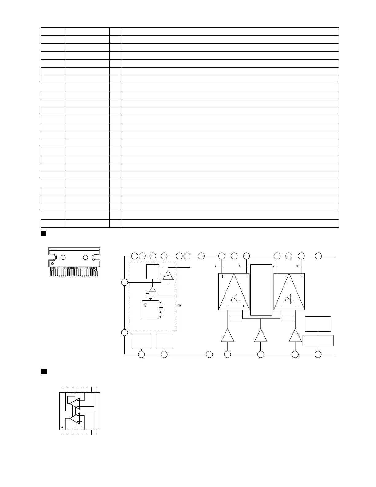
Pin No. Symbol I/O Function
8
Standby
SW
Switching regulator
block
CH 1
ON MUTE
muting circuit
Nonlinear amplifier/output
stage
Power supply/ground
shorting protection circuit
Overvoltage/thermal
protection circuit
BEEP
amplifier
Input
amplifier
AB D
C
Nonlinear/output stage
Amplifier
output
stage
SW
drive
D
C
B
A
H.L.S.
ST-BY RF PREGND IN 1 IN 2 ON-TIMEBEEP
VH
VH
SWB VL VL
SW
GND
+OUT1 +OUT2 NC-OUT1 -OUT 2PG1 PG2
H.L.S. :
Higher
Level signal
selector
Ripple
filter
LA4905 (IC301) : 2ch BTL power IC
1. Terminal layput 2. Block diagram
123
9 15 14 12 13 16 7 5 6 18 19 17 22
2314322021
10
11
Input
amplifier
CH 2
Pop noise
prevention
circuit
C
NJM4580D-D (IC101,IC211,IC212,IC213) : Dual operational amplifier
1. A OUTPUT
2. A -INPUT
3. A +INPUT
4. V
-
5. B +INPUT
6. B -INPUT
7. B OUTPUT
8. V
+
1. Terminal layout & Block diagram
8 7 6 5
1 2 3 4
B
A
CVL
 Loading...