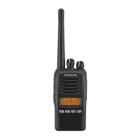
Do you have a question about the Kenwood NX-200 K2 and is the answer not in the manual?
Details copyright notices for the manual and embedded firmware.
Outlines manual's purpose and procedure for ordering replacement parts.
Crucial safety advice and notes on servicing the transceiver.
Flowchart detailing the steps from merchandise receipt to delivery.
Table showing frequency range, RF power, type, and DTMF keypad for models K and K2.
Explains different modes like User, PC, Clone, and their functions.
Table detailing modes and key combinations to enter them.
Details Panel Test, Panel Tuning, PC Mode, and Firmware Programming modes.
Steps for programming transceivers and transferring data via clone mode.
Procedure to check firmware version by holding a specific key during power-on.
Step-by-step guide to install the VGS-1 unit in the transceiver.
Do not remove black sheet or damage orange packing material for waterproofing.
Procedures for removing option PCB and installing VGS-1 components.
Steps for removing TX-RX unit and TOP packing, highlighting screw removal and FPC disconnection.
Mounting chassis onto the case and ensuring key tops fit correctly.
Procedures for handling lithium cell, keyboard ASSY, switches, and FPCs.
Procedure for installing relay hardware to the chassis.
Changing channel selector from 16-channel to free operation.
Explains which sheets/cushions to change with main parts for performance.
Notices for replacing units, firmware compatibility, and PCB compatibility.
Adjustment items need readjustment after unit replacement.
Description of transceiver components and frequency configuration.
Detailed description of RF and IF circuits, including filters and mixers.
Audio processing, filtering, mute switch, and speaker switching.
Amplifies demodulated noise, converts to DC signal for detection.
Covers audio band and base band circuits for transmission.
Details VOX, drive/final amplifier, and APC circuits.
Describes PLL, VCTCXO, and VCO circuits.
Describes the control circuit and the ASIC's functions.
Describes memory, LCD control, and key detection circuits.
Details low battery warning and DSP circuit functions.
Details battery voltage distribution, DC/DC conversion, and power supply control.
Describes signaling and compander circuits.
Lists ICs, transistors, LEDs, and diodes with their part numbers and descriptions.
Lists ICs, transistors, diodes, and other components for the TX-RX unit.
Detailed list of parts for the control unit, including part numbers and descriptions.
Continuation of the control unit parts list with component details.
Detailed listing of resistors and connectors for the control unit.
Continuation of the control unit parts list, focusing on resistors.
Final part of the control unit parts list, including variable resistors and diodes.
Includes diodes, ICs, and transistors for the control unit.
Lists components for the TX-RX unit, including diodes, ICs, and transistors.
Continues TX-RX unit parts list, focusing on capacitors.
Continues capacitor list and starts listing inductors and fuses for TX-RX unit.
Lists inductors, crystals, and resistors for the TX-RX unit.
Continues the resistor list and includes variable resistors and diodes for the TX-RX unit.
Lists diodes, ICs, and transistors for the TX-RX unit.
Visual representation of the transceiver's components and their assembly.
Illustrates how to pack the transceiver and accessories for shipping.
Flowchart for determining BGA IC issues when transceiver doesn't power on.
Verifies power supply voltages and control signals for troubleshooting.
Checks SBC and /LCDRST signals from ASIC for abnormalities.
Interprets LCD error messages like "INIT ERROR1", "INIT ERROR2", "INIT ERROR3".
Information on replacing control units and confirming original/service units.
Details service control unit data, labels, and PCB replacement steps.
Notes on ESN validation, NXDN Trunking, and Kenwood ESN changes.
Explains key functions for sub LCD display and panel test mode.
Table of frequencies and adjustments for various modes.
Lists specific frequencies for CH 1-6 and 7-16 for testing.
Configuration for analog and NXDN signaling modes.
Preparations and steps for entering transceiver tuning mode.
Detailed description of each adjustment item, its purpose, and conditions.
Maps adjustment items to LCD display, adjustment range, and item number.
Visual guide for performing adjustments in panel tuning mode.
Continues the flow chart for panel tuning mode adjustments.
Lists necessary equipment like SSG, power meter, oscilloscope for alignment.
Information on antenna connector adapters and nut wrench for adjustments.
Instructions for connecting and using the battery jig, including Li-ion battery detection.
Pin assignments for the universal connector used for tuning.
Connecting wires to PCB for PC tuning and processing the connector case.
Procedures for frequency, high power, low power, and MIC sensitivity checks.
Setting battery voltage, SSG modulation, and adjusting volume levels.
Adjusting VCO lock voltage for receive and real-time clock frequency.
Performing frequency adjustment only in PC test mode under specific conditions.
Adjusting high and low transmit power levels.
Adjusting balance and maximum deviation for NXDN.
Adjusting maximum deviation for NXDN (very narrow) and Analog (narrow/wide).
Adjusting QT deviation for Analog (narrow) and Wide modes.
Adjusting deviation for DQT, LTR, and DTMF signaling.
Adjusting deviation for single tone, MSK, and CWID.
Adjusting VOX sensitivity levels (VOX1 and VOX10).
Table of necessary deviation adjustments and battery detection/check procedures.
Adjusting AF level and sensitivity 1 for the receiver.
Adjusting sensitivity 2 and RSSI reference levels.
Adjusting open squelch levels for analog and NXDN modes.
Adjusting low RSSI levels at -118dBm for analog and NXDN.
Adjusting high RSSI levels at -80dBm for analog and NXDN.
Adjusting tight squelch levels for analog modes.
Details pin assignments and functions for connectors CN1, CN23, CN403, CN404.
Pin functions for TX-RX unit connectors CN405, CN701, CN710 and option board CN736.
Signal types and rating conditions for solder pads like PTT, MDSW, TXD, RXD, RSSI.
Details pin functions and ratings for the universal connector.
Detailed input/output, parameter, and rating conditions for CN710.
Continues the specification for the CN710 connector.
Pin assignments and functions for the CN736 option board connector.
Continues the specification for the CN736 option board connector.
Component side view of the control unit PC board with component references.
Component side view of the control unit PC board with component references.
Foil side view of the control unit PC board with component references.
Foil side view of the control unit PC board with component references.
Component side view of the TX-RX unit PC board with component references.
Component side view of the TX-RX unit PC board with component references.
Component side view of the TX-RX unit PC board (B/2) with component references.
Foil side view of the TX-RX unit PC board (A/2) with component references.
Shows connections between major PCB units and connectors.
Shows connections between Cord Assy, TX-RX PCB, Switch Unit, and ANT.
Detailed schematic of the control unit's circuitry.
Continuation of the control unit schematic, detailing ICs and connections.
Continuation of the control unit schematic, showing ASIC, DSP, and related circuits.
Final part of the control unit schematic, detailing various control and I/O signals.
Details power supply circuits and connections to option boards.
Details audio amplifier, squelch, and transmitter circuits.
Details audio amplifier, transmitter, and power supply circuits.
Continues the schematic for control unit, showing voltage regulators and switch units.
Details power supply circuits and connections to the TX-RX unit.
Continues the schematic showing power supply, voltage regulators, and connections to option boards.
Schematic of the TX-RX unit, showing RF and IF circuits.
Continuation of TX-RX unit schematic, detailing VCO, PLL, and receiver sections.
Continuation of TX-RX unit schematic, showing drive, final, and APC circuits.
Final part of TX-RX unit schematic, detailing antenna switch and other components.
High-level overview of the control unit's functional blocks and connections.
Functional blocks and connections for the TX-RX unit.
Continuation of TX-RX unit block diagram, showing circuits like PLL, VCO, and RF amplifier.
Final part of TX-RX unit block diagram, showing transmitter and receiver sections.
Shows signal levels in receiver and transmitter sections for measurements.
External views, specifications, and schematic diagrams for KNB-47L and KNB-48L batteries.
Covers models, frequency range, channels, zones, dimensions, and weight.
Details receiver sensitivity, selectivity and transmitter power, distortion.
| Brand | Kenwood |
|---|---|
| Model | NX-200 K2 |
| Category | Transceiver |
| Language | English |


