www.lairdtech.com/bluetooth
14
© Copyright 2018 Laird. All Rights Reserved
Americas: +1-800-492-2320
Europe: +44-1628-858-940
Hong Kong: +852 2923 0610
The coin cell powers only the BL654 module directly via SW6 (on the development board – power domain VDD_nRF_SW)
and through R46 provides power to the I2C RTC chip (U16).
Refer to the Appendix for the correct method of coin cell insertion and removal.
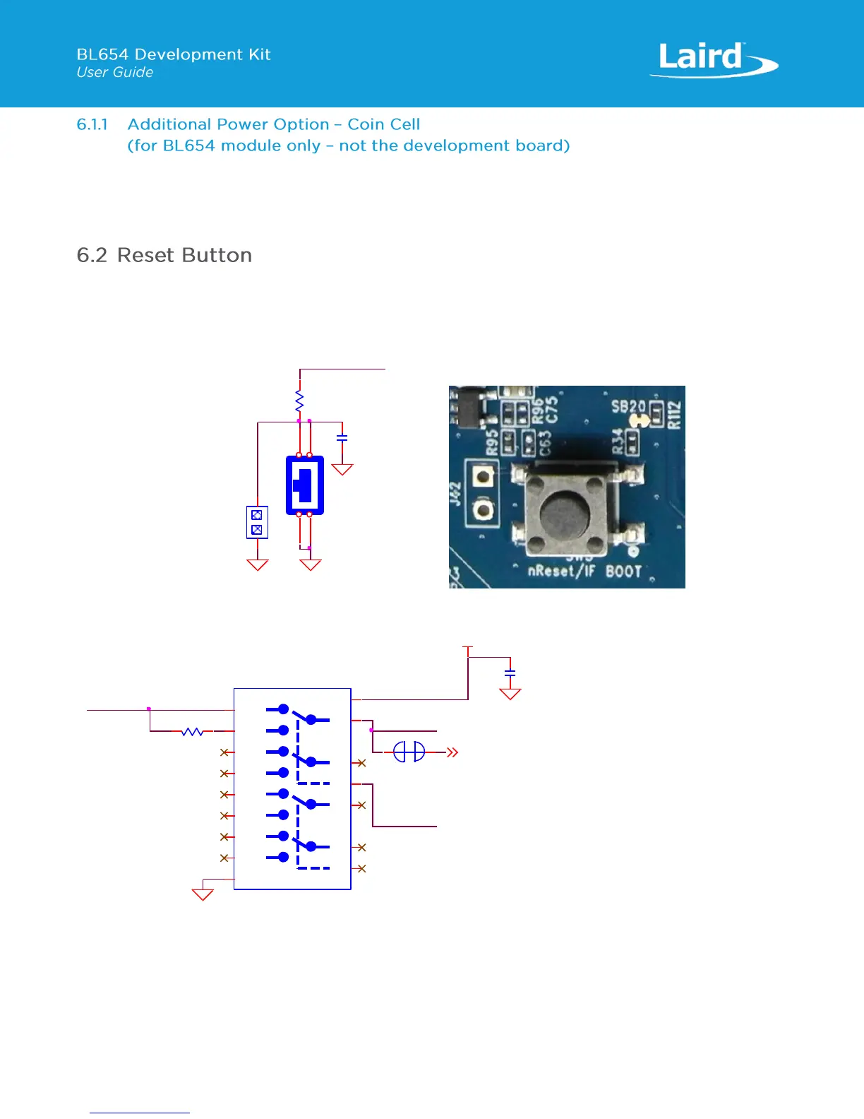
The development board has a reset button (SW3) with the net name BOOT_RESET_BLE. The BOOT_RESET_BLE (is active
low when SW3 pushed down) is routed to the BL654 module nRESET_BLE pin via an analog switch U25. The placement of
the Reset button is shown in Figure 6.
Figure 6: Reset button placement
Figure 7: Reset button schematic and routing through analog switch and location diagram
By default, whether the analog switch (U25) control line (USB_DETECT) is low (USB2 cable not plugged in) or high (USB2
cable plugged in), the nReset button (SW3) is routed via the analog switch (U25) to BL654 nReset pin (nRESET_BLE).
C63
NOPOP (0.01uF,16V)
GND
NOPOP (PIN HEADER,2.54mm 1X2P)
J42
1
1
2
2
GND
R34
150R
Reset
SW3
TACT SW,SMD/180d
1
1
2
2
3
3
4
4
BOOT_RESET_BLE
GND
SB22
NOPOP (Solderbridge)
1
1
2
2
BOOT_RESET_BLE
IMCU_BOOT
R1140R
VDD_VSRC_nRF
U25
Dual DPDT,1.65V~4.45V
1B0
1
1B1
15
2B0
5
2B1
3
1A
16
2A
4
1S
2
3B0
9
3B1
7
4B0
13
4B1
11
3A
8
4A
12
2S
10
GND
6
VCC
14
nRESET_BLE
GND
USB_DETECT
GND
C79
0.1uF,16V
 Loading...