The development board has USB2 cable detection circuit that generates the USB_DETECT signal on its output, so if a USB
cable is plugged into connector USB2, then USB2 cable detection circuit generates a HIGH on USB_DETECT or LOW if USB2
cable is not plugged in.
Table 3 displays the routing of SW3 reset button via analog switch U25 to the BL654 reset pin (regardless of whether the
USB cable is plugged into USB2 or not).
Table 2: USB U4 USB-SWD to BL654 SWD signal routing connections
R114 0R resistor if removed allows
SW3 to be disconnected from BL654
reset pin when USB2 cable plugged in.
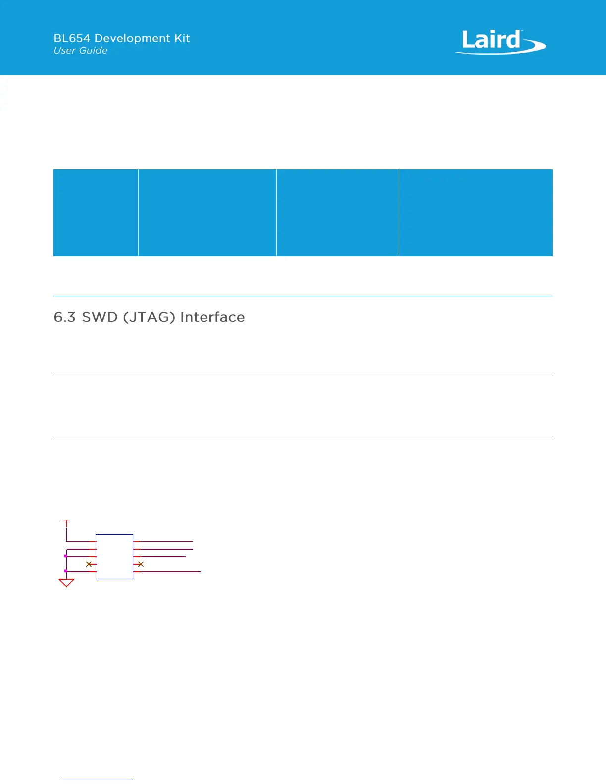
The development board provides access to the BL654 module two-wire SWD interface on JP1 via analog switch U24. This is
REQUIRED for customer use, since the BL654 module supports smartBASIC runtime engine firmware over JTAG (as well as
over UART).
Note: We recommend that you use JTAG (two-wire interface) to handle future BL654 module firmware upgrades. You
MUST wire out the JTAG (two-wire interface) on your host design (four lines should be wired out, namely SWDIO,
SWDCLK, GND, and VCC). Firmware upgrades can still be performed over the BL654 UART interface, but this is
slower (60 seconds using UART vs. 10 seconds when using JTAG) than using the BL654 JTAG (two-wire interface).
Upgrading smartBASIC runtime engine firmware or loading smartBASIC applications also can be done using the UART
interface.
For those customers (using Nordic SDK) that require access to BL654 SWD (JTAG) interface, the BL654 development board
(see Figure 1) has on-board circuitry to allow access to BL654 module SWD interface (via USB connector USB2).
Figure 9 shows the SWD on-board circuitry routing via analog switch U24
When the USB cable is plugged into connector USB2 (the USB cable detection output generates a HIGH for USB_DETECT and
USB_DETECTp when switch SW11 is in position 2-1 – the default) and Atmel MCU SWD (JTAG) signals are routed to the
BL654 SWD interface. This is required to connect the two-wire SWD (JTAG) interface from U14 to the BL654 SWD (JTAG)
interface.
When the USB cable is plugged into connector USB2 and the SW11 is in position 2-3 (Low), there is a LOW on U24 control
line USB_DETECTp and the Atmel MCU SWD (JTAG) signals are routed to connector JP1 (which is not populated).
 Loading...