EasyManua.ls Logo

Laird BL654 - Page 32

Laird BL654
38 pages
Print Icon
To Next Page IconTo Next Page
To Previous Page IconTo Previous Page
Loading...
www.lairdtech.com/bluetooth
32
© Copyright 2018 Laird. All Rights Reserved
Americas: +1-800-492-2320
Europe: +44-1628-858-940
Hong Kong: +852 2923 0610
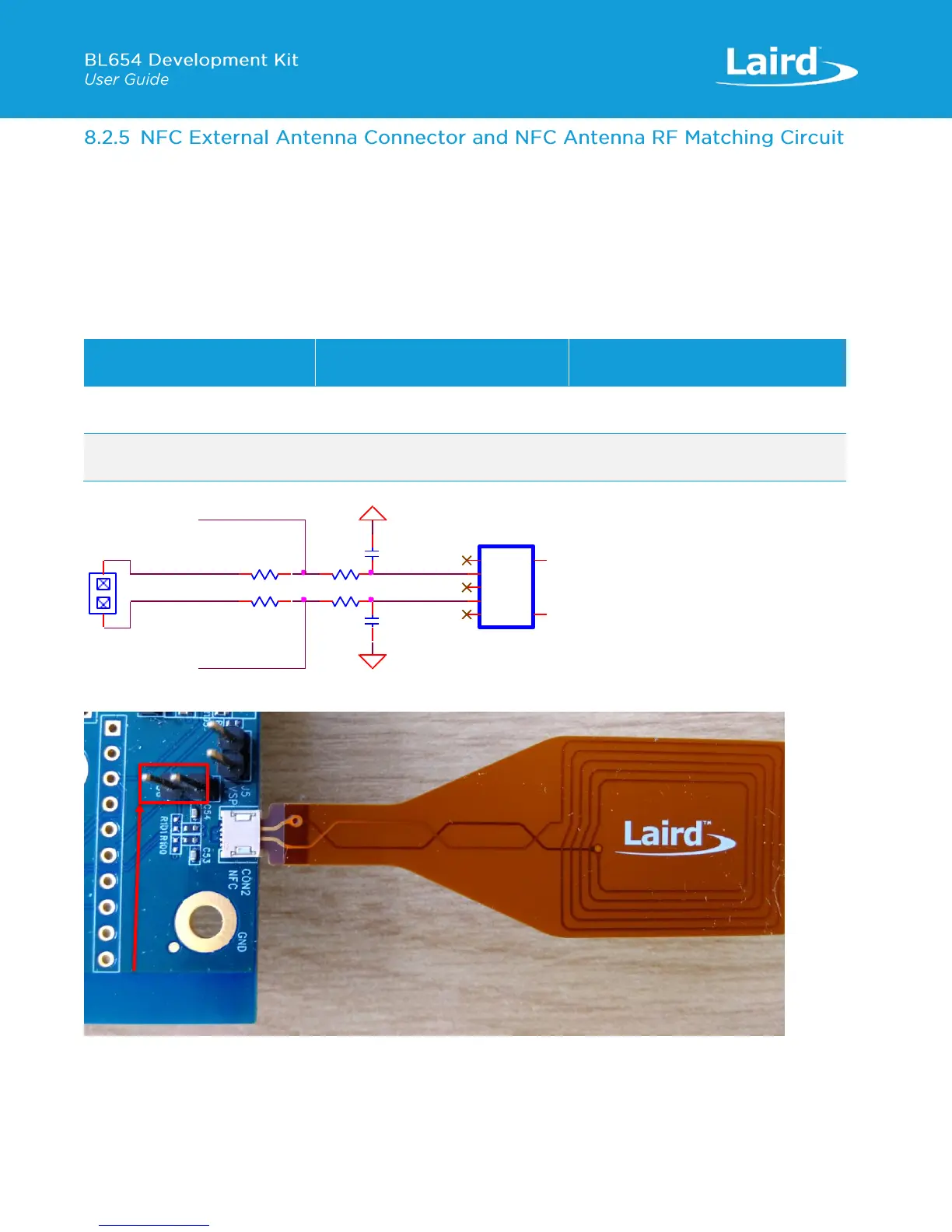
The NFC antenna input connector (CON2) allows the Laird supplied flex-PCB NFC antenna to be plugged in. The BL654
module NFC circuit uses two pins, pin 59 (NFC1/SIO_9) and pin 57 (NFC2/SIO_10) to connect the antenna. These pins are
shared with GPIOs (SIO.09 and SIO.10). BL654 NFC pins are enabled by default. NFC can be disabled via smartBASIC
application. Pin 59 (NFC1/SIO_9) and pin 57 (NFC2/SIO_10) are configured by default on the development board schematic
to use NFC antenna, but if pin 59 (NFC1/SIO_9) and pin 57 (NFC2/SIO_10) are needed as normal GPIOs, R98 and R99 must
be removed and R100 and R101 must be shorted by 0R.
C53 (300pF) and C54 (300pF) are RF tuning elements for the flexi-PCB NFC antenna.
Table 14: NFC input BL654 SIO signal mappings
BL654 (U5) SIO
Bring out SIO_9 and SIO_10 to NFC
antenna connector (CON2)
Bring out SIO_9 and SIO_10
to Header connector (J36)
pin 59 (NFC1/SIO_9)
Fit R98 0R (default)
Remove R100 0R (default)
Remove R98 0R
Fit R100 0R
pin 57 (NFC2/SIO_10)
Fit R99 0R (default)
Remove R101 0R (default)
Remove R99 0R
Fit R101 with 0R
Figure 18: NFC antenna RF matching circuit, NFC antenna connector schematic and NFC plugged in to connector CON2
C53
300pF,50VR100NOPOP (0R)
R101NOPOP (0R)
C54
300pF,50V
GND
PIN HEADER,2.54mm 1X2P
J36
1
1
2
2
GND
R98
0R
CON2
FFC/FPC,SMD/90d
1
1
2
2
3
3
4
4
5
5
GND
6
GND
7
NFC1_SIO_09
R99
0R
NFC2_SIO_10
J36

Other manuals for Laird BL654

Related product manuals