3 3
3 3
3
❏❏
❏❏
❏
activity: it must turn on (red light) at the amplifier output signal clipping.
➭
CURRENT AND SHORT CIRCUIT SENSOR CHECK:CURRENT AND SHORT CIRCUIT SENSOR CHECK:
CURRENT AND SHORT CIRCUIT SENSOR CHECK:CURRENT AND SHORT CIRCUIT SENSOR CHECK:
CURRENT AND SHORT CIRCUIT SENSOR CHECK:
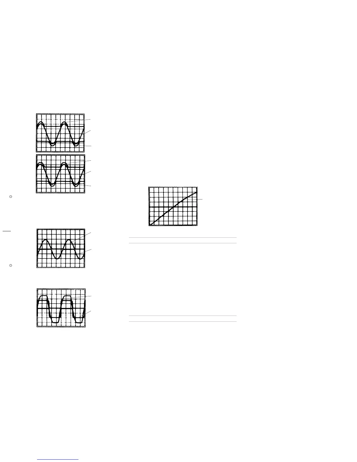
Set both the scope channels sensitivity to 0.5V/div., connect the scope
ch1 GND clip at CN3 pin 2 (AMP output) and the probe tip at TR106
(NPN) emitter, connect the ch2 probe tip at TR113 (PNP) emitter.
Set the generator to have approx. 1Vp on the emitters: their difference
must be less than 0.2V on the peaks (see
Fig.4 Trace A & B
).
Connect a 4Ω 500W load. Increase the input signal, the output current
limiter must keep the emitter voltages, both half channel, at 1.5Vp
approx. (see
Fig.5 Trace A
).
Temporarily short the amplifier output: the current limiter must keep the
emitter voltages (both half channel) at 1 approx. (see
Fig.5 Trace B
).
➭
OFFSET SENSOR CHECK:OFFSET SENSOR CHECK:
OFFSET SENSOR CHECK:OFFSET SENSOR CHECK:
OFFSET SENSOR CHECK:
Set the Variac to zero voltage output, disconnect the amplifier load and
the supply connection from the Power Supply & I/O Board (CN2-4), turn
on the amplifier, connect temporarily (by means of a suitable conductor
wire) CN2 pin 2 to +15Vdc (CN3 pin 5), the PROTECT led must turn on in
5 seconds approx.
Remove the connection, wait until the leds turn off and after some sec-
onds repeat the check with -15Vdc (available on CN3 pin 3), the led
PROTECT must turn on again.
➭
BIAS CHECK:BIAS CHECK:
BIAS CHECK:BIAS CHECK:
BIAS CHECK:
Disconnect ch2 probe. Connect the ch1 scope GND clip to CN2 pin 1
(GND terminal) and its probe tip to CN2 pin 2 (AMP output). Adjust the
generator level until the sinewave appears at full screen amplitude, no
crossover distortion must be detectable: if necessary re-adjust R132.
➭
BANDWIDTH CHECK:BANDWIDTH CHECK:
BANDWIDTH CHECK:BANDWIDTH CHECK:
BANDWIDTH CHECK:
Set ch1 scope sensitivity at 20V/div., increase the generator level to have
80Vpp, sweep the generator frequency from 20Hz to 20KHz: the output
level must have not detectable level changes.
➭
SLEW RATE CHECK:SLEW RATE CHECK:
SLEW RATE CHECK:SLEW RATE CHECK:
SLEW RATE CHECK:
Set the scope sensitivity to 10V/div. 1µS/div. and set the generator to
1KHz square wave mode. Check the output square wave rising and falling
edge slopes: both must be 10V/µS or more as shown in
Fig 6
.
Inputs & Protections Board CheckInputs & Protections Board Check
Inputs & Protections Board CheckInputs & Protections Board Check
Inputs & Protections Board Check
➭ These procedures are intended for one channel at a time, repeat these
operations for the other channel.
➭
SETUP:SETUP:
SETUP:SETUP:
SETUP:
Connect the ch1 probe to amplifier input of the channel under test and set
it at 500mV/div. 200mS/div.
Connect the ch2 probe to amplifier output of the channel under test and
set it at 10mV/div. 200mS/div.
Set the audio generator at 1KHz sinus. 775mV
RMS
(0dB).
Set the LEVEL potentiometers full clockwise.
The load resistor is disconnected.
➭
AMPLIFIER GAIN CHECKAMPLIFIER GAIN CHECK
AMPLIFIER GAIN CHECKAMPLIFIER GAIN CHECK
AMPLIFIER GAIN CHECK
Check the output levels: at 775mV position the output voltage must be
46±1.5Vp.
➭
SIGNAL TO NOISE RATIO CHECKSIGNAL TO NOISE RATIO CHECK
SIGNAL TO NOISE RATIO CHECKSIGNAL TO NOISE RATIO CHECK
SIGNAL TO NOISE RATIO CHECK
Disconnect the audio generator the output signal (noise) must be less
1mV.
AdvicesAdvices
AdvicesAdvices
Advices
➭ Check the channels one at time to determine which is right (note: if you
have a spare amplifier module that you know as right, use it).
➭ If you have determinate that the problem is a short on a rail, you must
check the output transistors.
To determine which transistor devices are bad, use a soldering iron to lift
Fig. 2Fig. 2
Fig. 2Fig. 2
Fig. 2
Fig. 3Fig. 3
Fig. 3Fig. 3
Fig. 3
Fig. 5Fig. 5
Fig. 5Fig. 5
Fig. 5
Trace A (0.5V/div.)
Trace B (0.5V/div.)
Fig. 4Fig. 4
Fig. 4Fig. 4
Fig. 4
Trace A (0.5V/div.)
Trace B (0.5V/div.)
one leg of each emitter pin and measure the emitter-collector resistance
on each device. Unsolder and lift one leg of each base pin and check the
base-collector resistance of each transistor and replace any that measure
as a short.
If all the transistors are OK, unsolder and lift one leg of each diode and
check them.
Check the circuit board for open foil traces.
Use the Multimeter as Ohm-meter to check the resistors, particularly the
base and emitter resistors of damaged transistor.
➭ If the input sinewave appears to be distorted during the negative cycle,
you can assume that the problem is located somewhere in the circuitry of
the positive low rail.
If the positive cycle appears distorted, you can assume that the problem
is in the circuitry of the negative low rail.
➭ If the high rails appear distorted or are not modulating as shown in figure,
then the problem probably exists somewhere in the circuitry of the re-
spective (+ or -) defective high rail. Refer to the schematics.
Fig. 6Fig. 6
Fig. 6Fig. 6
Fig. 6
Trace A (10V/div.)
Trace B (20V/div.)
Trace A (20V/div.)
Trace C (20V/div.)
Trace B (20V/div.)
Trace A (20V/div.)
Trace C (20V/div.)
 Loading...