Do you have a question about the LG LM-M530A/D/X and is the answer not in the manual?
Precautions for handling and servicing the optical pick-up unit.
Essential preparation and repair guidelines for CD player components.
Guidelines for safely handling Electrostatic Sensitive Devices (ESD).
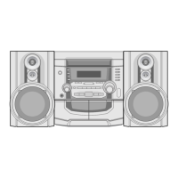
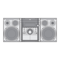
Technical specifications for the audio system's components and performance.
Procedures for factory alignment and adjustments for tape deck operation.
Method for adjusting record bias for tape deck functionality.
Step-by-step troubleshooting guide for CD player malfunctions.
Voltage sheet for CD part integrated circuits.
Key waveforms for diagnosing CD part functionality.
Layout diagram of the Power Printed Circuit Board.
Component layout of the CD Main Printed Circuit Board (Component Side).
Component layout of the CD Main Printed Circuit Board (Solder Side).
Internal block diagram and pin assignment for IC801.
Detailed pin descriptions for IC801.
Block diagram and pin definitions for BA5810FP (IC803).
Description and pin definitions for KA3082 (IC 804).
Electrical characteristics of KIA 78R12 voltage regulator.
Equivalent circuit diagram for KIA7805AP/API (IC 901).
Description of BA3126N (IC 201) as a 2-channel head switch.
Block diagram and pin description for BU2090F (IC 501).
Method for repairing distorted tray gears in the CD mechanism.
Overall system block diagram illustrating component interactions.
Main schematic diagram of the system's circuitry.
Schematic diagram for the front panel and associated circuits.
Schematic diagram for the tuner and tape deck sections.
Schematic diagram for the CD player section.
Wiring diagram illustrating interconnections between major assemblies.
Solder side layout of the Main Printed Circuit Board.
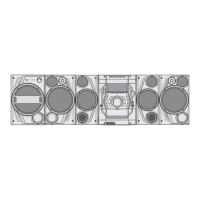
Exploded view of the cabinet and main frame assembly.
Exploded view of the optional auto stop tape deck mechanism.
Exploded view of the auto reverse tape deck mechanism.
Exploded view of the CD mechanism.
| Brand | LG |
|---|---|
| Model | LM-M530A/D/X |
| Category | Stereo System |
| Type | Mini Hi-Fi System |
| Number of Discs | 1 |
| Audio Output Mode | Stereo |
| Tuner Bands | FM |
| Remote Control | Yes |
| Speaker Type | 2-Way |
| Bluetooth | Yes |
| USB Port | Yes |
| FM Radio | Yes |
| AUX Input | Yes |
| Playable Media | CD-R, CD-RW |
| Weight | 3.5 kg |