114-5
DSP BOARD 114 REV C
©1998 Mackie Designs Inc. All rights reserved
C91
C89
C40
C60
C36
C67
C179
C79
C102
C218
C104
C237
C115
C238
C136
C235
C149
C167
C153
C225
C131
C227
C138
C207
C97
C83
C28
C88
C185
C73
C169
C76
C177
C217
C101
C120
C161
C125
C113
C236
C150
C175
C147
C226
C181
C228
C121
C239
C99
C34
C43
C245
C68
C244
C170
C92
C85
C93
C116
C39
C132
C243
C148
C96
C46
C157
C183
C240
C214
C241
C212
C242
C51
C38
C27
C195
C186
C202
C107
C208
C176
C211
C106
C126
C114
C143
C160
C224
C154
C193
C146
C230
C197
C229
C139
C233
C48
C192
C53
C201
C187
C203
C171
C209
C178
C210
C105
C124
C163
C173
C162
C219
C155
C194
C180
C231
C145
C232
C144
C234
C45
C90
C65
C62
C59
C75
C58
C74
C57
C81
C66
C82
C158
C134
C52
C159
C47
C190
C168
C174
C42
C206
C44
C222
12 17 41 60 66 92
15 18 36 59 67 90
7
14
10
20
10
20
C98
C56
C72
C95
C100
C111
C133
C152
C165
C184
C200
C191
C49
C246
C54
C61
C69
C78
C86
C94
C110
C29
C119
C109
C117
C142
C166
C141
C182
C172
C198
C188
C215
C205
C213
C216
C50
C37
C55
C63
C70
C71
C84
C77
C103
C87
C118
C127
C135
C140
C151
C156
C164
C17
C199
C189
C196
C204
C223
C221
U1
U2
U3
U4
U5
U6
U7
U8
U9
U10
U11
U12
U13
U55
U49
U53
U59
U62
U65
U68
U56
U44
U50
U57
U60
U63
U66
U69
U72
U75
U78
U81
U84
U54
U26
U39
U51
U58
U61
U64
U67
U70
U73
U76
U79
U82
U14
U15
U16
U17
U18
U19
U20
U21
U22
U23
U24
GND
PIN
+5v
PIN
GND
PIN
+5v
PIN
GND
PIN
+5v
PIN
GND
PIN
+5v
PIN
U71
U74
U77
U80
U83
U87
U90
U93
U96
U99
U102
U105
U108
U111
U114
U117
U85
U88
U91
U94
U97
U100
U103
U106
U109
U112
U115
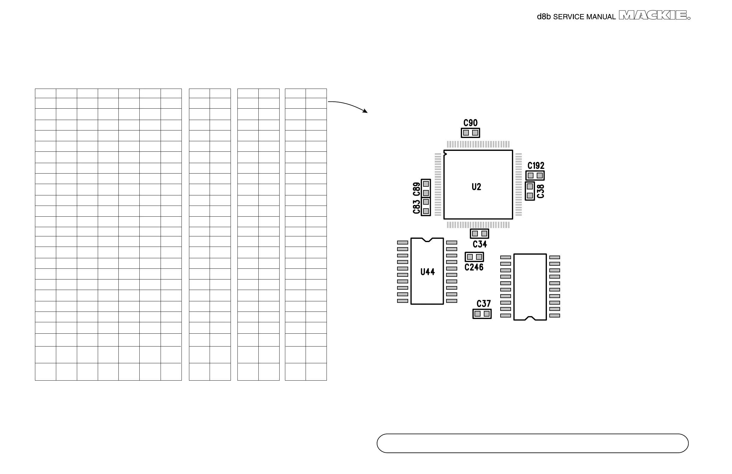
These are the bypass capacitors for each IC (reading along the row), connected between ground and +5volts.
The schematic on sheet 3 shows the location of the caps for U1, U55, U56 and U54.
The portion of the PCB shown on this page is for U2, U44 and U26. The caps are grouped in the same pattern
for most of the 24 repeats.
Look in the table to find the caps for other ICs.
You can also see which ICs go together, for example, U1 is used with U55, U56 and U54, reading along the row.
This pattern is repeated 24 times
U26
 Loading...