2-27
Pin No. Port Name I/O FUNCTION
166 DA-LRCK O PCM left/right clock. Identifies the channel for each audio sample.
167 DA-BCK O PCM bit clock output.
169 DA-XCK I/O Audio master frequency clock.
171 DAI-DATA I PCM input DATA (not used).
172 DAI-LRCK I PCM input LRCK (not used).
173 DAI-BCK I PCM input BCK (not used).
175 CLKSEL I Clock select pin. (H: internal, L: external)
176 A-VDD Ð +3.3 V power supply for analog section.
177 VCLK O Video clock. (27 MHz)
178 SYSCLK I System clock input. Decoder requires an external 27 MHz TTL oscillator.
179 A-VSS Ð Analog ground for PLL.
180
DVD-DATA0
I Serial CD data.
/CD-DATA
182
DVD DATA1
I DVD DATA1 input or CD-LRCK input.
/CD LRCK
184
DVD-DATA2
I DVD DATA2 input or CD bit clock input.
/CD BCK
185
DVD-DATA3
I DVD DATA3 input. Asserted HIGH indicates a corrupted byte.
/CD-C2PO
186-189
DVD-DATA4-7
I
DVD parallel compressed data from DVD DSP or
CDG 4-7 CDG-SDATA/ VSFY/S0S1/SCLK signal input.
191 VREQUEST O
Video request. Decoder asserts VREQUEST to indicate that the video input
buffer has available space.
192 VSTROBE I Video strobe signal input.
194 AREQUEST O
Audio request. Decoder asserts AREQUEST to indicate that the audio input
buffer has available space.
196 V-DACK I Video data acknowledge (in synchronous mode). Asserted when DVD is valid.
198 A-DACK I Audio data acknowledge.
200 ERROR I
Error in input data. If error signal is not available from the DSP, it must be
grounded.
202-204 HADDR0-2 I Host address bus. 3-bit address bus selects one of eight host interface registers.
205 DTACKSEL I
Tie HIGH to select WAIT signal, LOW to select DTACK signal.
(Motorola 68 K mode)
206 CS I
Host chip select. Host asserts CS to select the decoder for a read or write
operation.
207 R/W I
Read/write strobe in M mode. Write strobe in I mode.
Host asserts R/W LOW to select write and LOW to select read.
208 RD I Read strobe in I mode. Must be held HIGH in M mode.
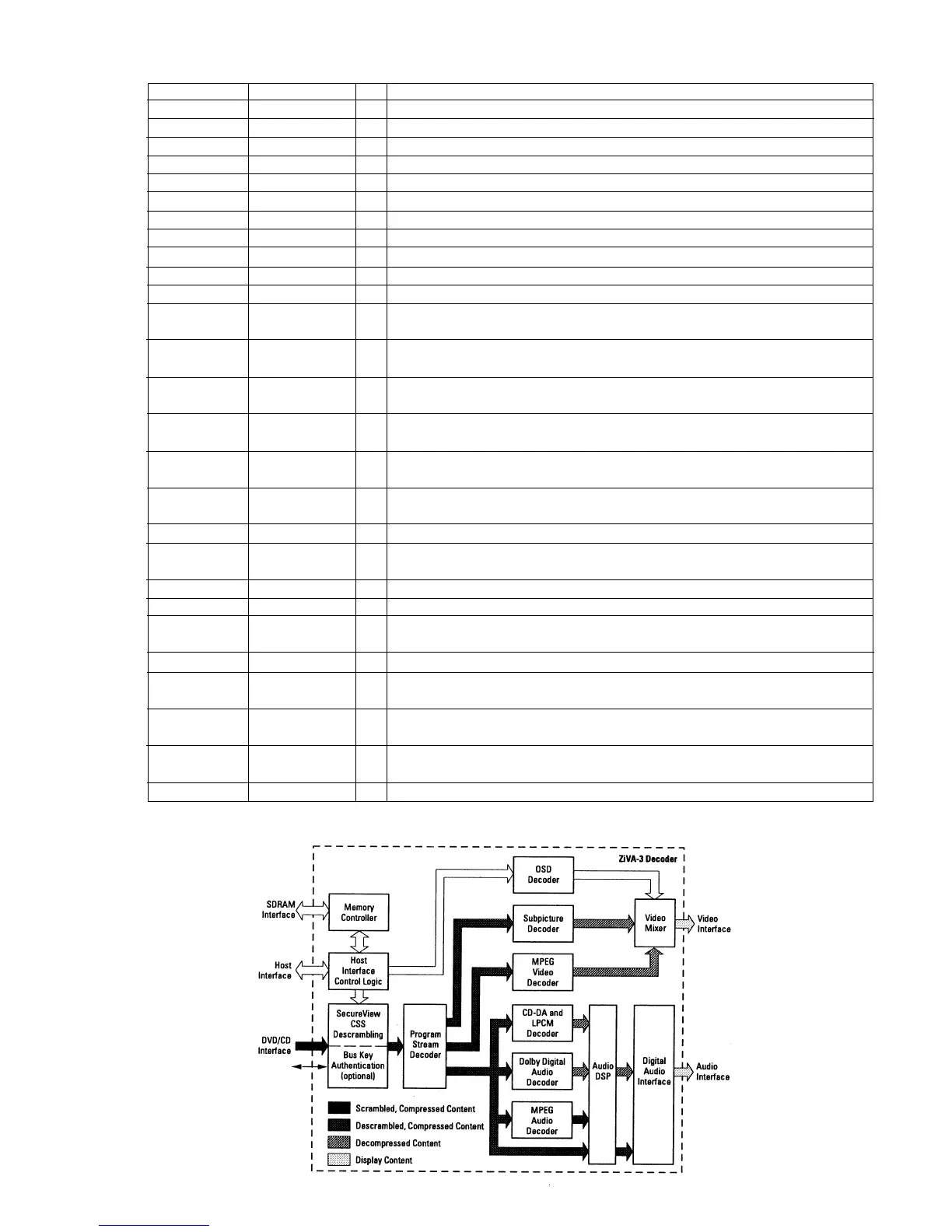
ZIVA-3 (MPEG AV decoder)