EasyManua.ls Logo

MSI ms 7529 User Manual

MSI ms 7529
33 pages
To Next Page IconTo Next Page
Page #1 background imageLoading...
Page #1 background image
1
1
A A
Size Document Description Rev
Sheet of
Date:
MSI
1.1
MS-7529
133
Custom
Cover Sheet
Friday, May 16, 2008
MICRO-STAR INT'L CO.,LTD
Size Document Description Rev
Sheet of
Date:
MSI
1.1
MS-7529
133
Custom
Cover Sheet
Friday, May 16, 2008
MICRO-STAR INT'L CO.,LTD
Size Document Description Rev
Sheet of
Date:
MSI
1.1
MS-7529
133
Custom
Cover Sheet
Friday, May 16, 2008
MICRO-STAR INT'L CO.,LTD
MS-7529
System Chipset:
Expansion Slots:
CPU:
On Board Chipset:
PCI2.3 SLOT * 2
BIOS -- SPI
HD -- ALC888
LPC Super I/O -- F71882FG
Intel Bearlake - MCH (North Bridge)
Intel ICH7R (South Bridge)
Main Memory:
ST PWM:
Controller: 3 PHASES
PCI EXPRESS X16 SLOT
1Cover Sheet
Block Diagram/Clock Map/Power Map
2-4
CLOCK -- RTM876-665
LAN-- REALTEK RTL8111C Co-lay RTL8101E
Version 1.1
ATA33/66/100 IDE & SATA Connectors
Azalia - ALC888
12
Intel ICH7 - LPC & ATA & USB & GPIO 13
Intel ICH7 - PCI & DMI & CPU & IRQ
5-7
Clock - RTM 876-665
PWM-ST L6703TR
USB Connectors
ATX Connetcor & Front Panel
Intel LGA775 CPU
UPI ACPI CONTROLLER
22
21
LPC I/O - Fintek 71882FG
PCI Slot 1 & 2
GMCH VCORE
DDR II VTT Decoupling
PCI EXPRESS X16 Slot
Intel Bearlake - MCH
Intel ICH7 - POWER
23
8-11
14
15
16
17
18
19
20
LAN REALTEK RTL8111C/8101E
24
25
26
27
28
29
30
DDR II DIMM A
DDR II *2 (Max 4GB)
VGA Connector
Intel Conroe (65W Dual core)
DDR II DIMM B
Question and Answer IconNeed help?

Do you have a question about the MSI ms 7529 and is the answer not in the manual?

MSI ms 7529 Specifications

General IconGeneral
Socket TypeLGA 775
Number of Memory Slots2
PCI Express x16 Slots1
PCI Slots2
IDE Ports1
Form FactorMicro ATX
ModelMSI MS-7529
SATA Ports4
USB Ports8
AudioRealtek ALC888

Summary

System Block Diagram

Intel LGA775 Processor Block

Diagram showing the Intel LGA775 CPU and its main connections.

Bearlake GMCH Block

Block diagram illustrating the Bearlake GMCH (North Bridge) chipset.

ICH7 Block

Block diagram illustrating the ICH7 (South Bridge) chipset.

Power Delivery and Voltage Regulators

Processor Power Supply

Details voltage regulators and power delivery for the CPU.

Chipset Power Circuits

Power supply configurations for MCH and ICH chipsets.

Intel ICH7: PCI, DMI, CPU & IRQ Interfaces

PCI Interface Pin Assignments

Detailed pinout for the PCI interface on the ICH7.

Intel ICH7: LPC, ATA, USB & GPIO Ports

LAN Controller Realtek RTL8111C/8101E

DDR II DIMM A Interface Details

DDR II DIMM A Pinout

Detailed pin assignments for DDR II DIMM slot A.

DDR II DIMM B Interface Details

DDR II DIMM B Pinout

Detailed pin assignments for DDR II DIMM slot B.

PCI Express X16 Slot Pinout

PCI Slots 1 and 2 Pinouts

ATX Connector and Front Panel Connectors

Core and DDR Memory Power Delivery

DDR II 1.8V Power Supply

Power supply circuit for DDR II memory modules.

1.5V Core Power Supply

Power delivery circuit for the 1.5V core voltage rail.

Voltage Regulator Module (VRM) Circuitry

L6703TR VRM Controller Details

Details of the L6703TR PWM controller for voltage regulation.
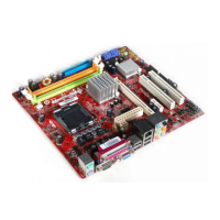
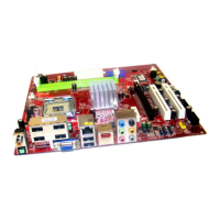
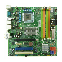
ICH7 GPIO and Configuration Details

Related product manuals