Appendix B Timing Diagrams
© National Instruments Corporation B-23 M Series User Manual
Figure B-23. Input Timing Diagram
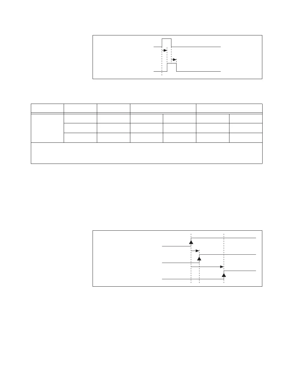
Internal Analog Output Timing
The analog output timer has two internal clocks that are
referenced—Sample Clock Timebase and Sync Sample Clock Timebase.
How they are generated depends on how the analog output timer is
configured. If the analog output timing engine is configured to operate with
an external Sample Clock, analog output internal clock timing can be
derived from Table B-13.
Figure B-24. External Update Source Clock Insertions Timing Diagram
Table B-12. Input Timing
Time From To Min (ns) Max (ns)
t
1
*
PFI PFI_i 4.1 6.4 15.2 19.2
RTSI RTSI_i 0.9 2.2 2.0 3.0
STAR STAR_i 0.9 — — 2.8
*
The delay ranges given for PFI and RTSI represent the fastest and slowest terminal routing within the trigger group for a
given condition (maximum or minimum timing). This difference can be useful when two external signals will be used
together and the relative timing between the signals is important.
Terminal
_i
t
1
t
1
Signal_i
Sample Clock Timebase
Sync Sample Clock Timebase
t
2
t
3
 Loading...