Appendix B Timing Diagrams
M Series User Manual B-30 ni.com
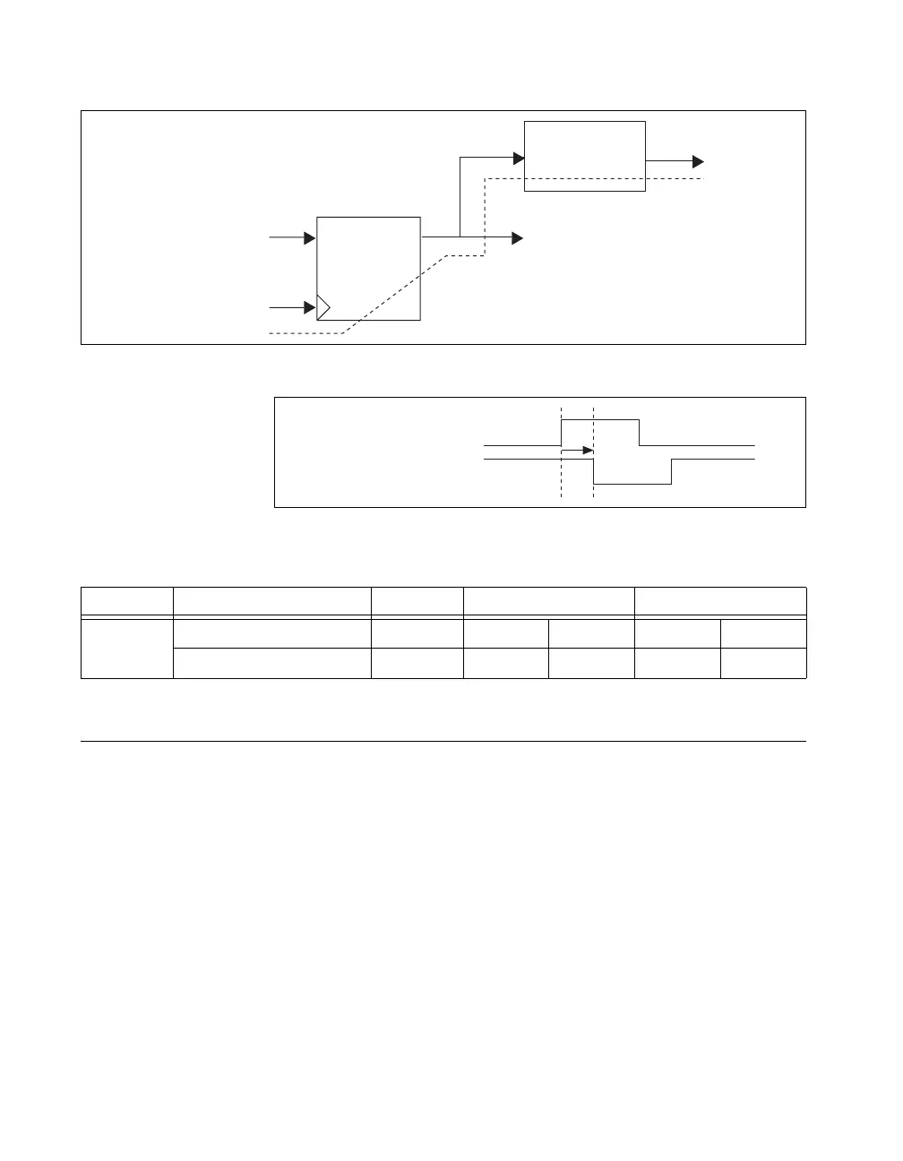
Figure B-35. Sample Clock Path
Figure B-36. Sample Clock Delay Timing Diagram
Digital I/O Timing Diagrams
This section describes the timing delays and requirements of digital
waveform acquisitions and digital waveform generations.
Digital Waveform Acquisition Timing
To describe digital waveform acquisition timing delays and requirements,
refer to the circuitry shown in Figure B-37. In the figure, P0, PFI, RTSI, and
PXI_STAR represent signals at connector pins of the M Series device. The
other named signals represent internal signals.
Table B-21. Sample Clock Delay Timing
Time From To Min (ns) Max (ns)
t
14
AO Sample Clock PFI 9.7 10.7 31.1 34.3
AO Sample Clock RTSI 8.8 9.1 21.3 21.7
Internal Logic
Sample Clock Timebase
D Q To Internal Logic
Routing Logic
RTSI, PFI
Sample Clock Timebase
RTSI/PFI Terminal
t
14
 Loading...