AND8344/D
www.onsemi.com
11
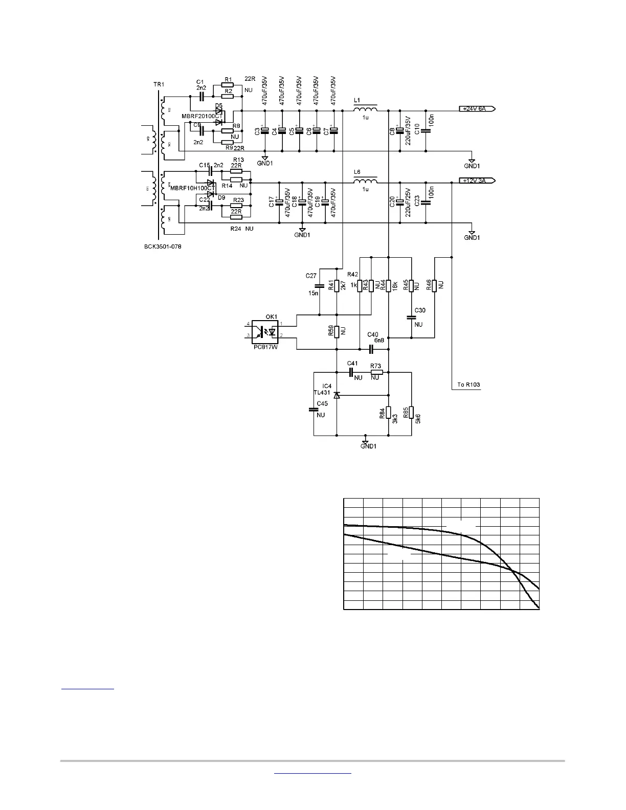
Secondary Side:
Figure 12. The LLC Secondary Side Schematic
The main LLC has two outputs, 24 V/6 A and 12 V/3 A.
The regulation loop is taken only from the 24 V line, but the
PCB is designed to accommodate a percentage weight of
both voltages if desired. In the default configuration, the
accuracy of the 12 V line is set only by the turns ratio of the
secondary windings. Alternate current from secondary
windings W2 and W3 of TR1 is rectified by double diode D5
and filtered by the set of capacitors C4, C5, C6, C7, C8, C10,
and L1 and connected to the output terminal. The voltage on
diode D5 is snubbed by RC segment R1, R9, C1 and C9 to
suppress overshoot on the diode. The output voltage is
divided by R44 and the parallel combination of R84 and
R85. IC4 is biased by resistor R42. Resistor R41 and
capacitors C27 and C40 comprise the compensation
network. To learn how to choose these devices and how to
arrange this circuit, please see application note
AND8327/D
. The Bode plot in this configuration is shown
in Figure 13.
Gain chart
−60
−50
−40
−30
−20
−10
0
10
20
30
40
50
60
0.1 0.2 0.3 0.5 0.8 1.3 2.2 3.6 6.1 10.2 17
Frequency [kHz]
Gain [dB]
−180
−150
−120
−90
−60
−30
0
30
60
90
120
150
180
Phase [°]
Figure 13. Frequency Response of the Open
Regulation Loop of the LLC
Phase
Gain
The 12 V line is accomplished by rectifying alternate
current from W4 and W5 windings of TR1 by double diode
D9. This diode is snubbed by R13, C15, R23 and C22.
 Loading...