EasyManua.ls Logo

Onkyo CR-305X Service Manual

Onkyo CR-305X
25 pages
To Next Page IconTo Next Page
Page #1 background imageLoading...
Page #1 background image
CD RECEIVER
MODEL CR-305X
Ref.NO.3654
082000
TABLE OF CONTENTS
CR-305X
Specifications -----------------------------------------------------------
Caution on replacement of optical pickup --------------------------
Protection of eyes from laser bam during servicing ---------------
Service procedures -----------------------------------------------------
Front panel view ------------------------------------------------------
Rear panel view -------------------------------------------------------
Remote controller ----------------------------------------------------
Microprocessor connection diagram --------------------------------
Microprocessor terminal descriptions ------------------------------
IC Block diagram and descriptions ---------------------------------
CD Mechanism exploded view --------------------------------------
Replacement of optical pickup ---------------------------------------
Chassis exploded view parts list -------------------------------------
Chassis exploded view -----------------------------------------------
Block diagram ---------------------------------------------------------
Wiring view ------------------------------------------------------------
Printed circuit board view parts list --------------------------------7
Schematic diagram (Amplifier section) -----------------------------
Printed circuit board view 1-------------------------------------------
Schematic diagram (CD & Microprocessor section) -------------
Printed circuit board view 2-------------------------------------------
Printed circuit board view 3-------------------------------------------
CD Adjustment procedures ------------------------------------------
Clock adjustment procedures ----------------------------------------
Assembling of pad ---------------------------------------------------
packing view ---------------------------------------------------------
2
2
3
4
5
6
7
8
9
10
19
21
22
23
25
26
27
29
31
33
35
37
39
40
41
42
Silver models
120 V AC,60 Hz
230 V AC,50 Hz
220 - 230 V AC,50/60Hz
UDD,UDT
UPP
UGT,UGR
SAFETY-RELATED COMPONENT WARNING!!
COMPONENTS IDENTIFIED BY MARK ON THE
SCHEMATIC DIAGRAM AND IN THE PARTS LIST
ARE CRITICAL FOR RISK OF FIRE AND ELEC-
TRIC SHOCK. REPLACE THESE COMPONENTS
WITH ONKYO PARTS WHOSE PARTS NUMBERS
APPEAR AS SHOWN IN THIS MANUAL.
MAKE LEAKAGE-CURRENT OR RESISTANCE
MEASUREMENTS TO DETERMINE THAT EXPO-
SED PARTS ARE ACCEPTABLY INSULATED FORM
THE SUPPLY CIRCUIT BEFORE RETURNING THE
APPLIANCE TO THE CUSTOMER.

Other manuals for Onkyo CR-305X

Question and Answer IconNeed help?

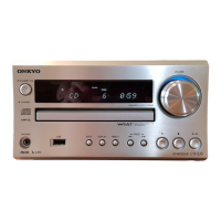
Do you have a question about the Onkyo CR-305X and is the answer not in the manual?

Onkyo CR-305X Specifications

General IconGeneral
CD PlayerYes
Channels2.0
Frequency Response20 - 20000 Hz
Playback FormatsCD-R, CD-RW
Tuner BandsFM

Summary

Safety-Related Component Warning

Specifications

Amplifier Specifications

Detailed specifications for the amplifier section, including power output and distortion.

Tuner Specifications

Detailed specifications for the tuner section, including tuning range and sensitivity.

CD Player Specifications

Detailed specifications for the CD player section, including signal readout and frequency response.

General Power and Dimensions

Information on power supply, consumption, dimensions, and weight of the unit.

Caution on Optical Pickup Replacement

Precautions for Optical Pickup Handling

Essential safety precautions for handling the optical pickup to prevent damage.

Laser Beam Protection During Servicing

Laser Diode Properties

Technical details of the laser diode used in the optical pickup.

Laser Warning Label Identification

Description and explanation of the laser warning labels affixed to the unit.

Service Procedures

Replacing the Fuses

Instructions on how to safely replace fuses, including identification and rating.

Initializing the Unit

Procedure to reset the unit to factory default settings and clear memory.

Safety-Check Out Procedure

Performing safety checks after repair, focusing on insulation resistance.

Memory Preservation Details

Information on the unit's built-in memory backup system and its behavior.

Changing the AM Band Step

Steps to modify the AM tuning step selector by changing specific resistors.

Microprocessor Connection Diagram

Microprocessor Terminal Description

IC Block Diagram and Descriptions

Terminal Description for Q101

Q301:CXD2589Q (CD Digital Signal Processor) Bloch Diagram

Terminal Description for Q301

Analog Function Switch Block Diagrams

Q401: TC9273N-007 Analog Function Switch

Block diagram and pinout for the TC9273N-007 analog function switch IC.

Q402: TC9162AF Analog Function Switch

Block diagram and pinout for the TC9162AF analog function switch IC.

Driver and Decoder IC Block Diagrams

Q102: LA6541D (4-channel Driver)

Block diagram and pinout for the LA6541D 4-channel driver IC.

Q180: BU1923 (RDS Decoder)

Block diagram and pinout for the BU1923 RDS decoder IC.

Motor Driver and Inverter IC Block Diagrams

Q103: TA7291S (Motor Driver)

Block diagram and pinout for the TA7291S motor driver IC.

Q691: TC7WU04FU (Triple Inverters)

Block diagram and pinout for the TC7WU04FU triple inverter IC.

CD Mechanism Exploded Views

CD Mechanism Exploded View (1)

First part of the exploded view showing CD mechanism components.

CD Mechanism Exploded View (2)

Second part of the exploded view showing CD mechanism components.

Replacement of Optical Pickup

Optical Pickup Replacement Steps

Step-by-step instructions for replacing the optical pickup.

Chassis Exploded View Parts List

Chassis Exploded View

Block Diagram

Wiring View

Printed Circuit Board View Parts List

Schematic Diagram (Amplifier Section)

Printed Circuit Board View 1

U2 Power Supply PC Board

Component layout for the power supply PC board (NAPS-6878).

U1 Selector Circuit PC Board

Component layout for the selector circuit PC board (NAAF-6874).

Printed Circuit Board View 1 (Cont.)

U5 Speaker Terminal PC Board

Component layout for the speaker terminal PC board (NAETC-6881).

U6 Digital Output PC Board

Component layout for the digital output PC board (NAETC-6882).

Chassis Exploded View Parts List (Cont.)

Printed Circuit Board View 3

U9 Connector PC Board

Component layout for the connector PC board (NAETC-6883).

U4 Power Amplifier PC Board

Component layout for the power amplifier PC board (NAAF-6880).

CD Adjustment Procedures

Focus Gain Adjustment

Procedure for adjusting the focus gain for optimal CD playback.

Clock Adjustment Procedures

Packing View

Assembling of Pad

Related product manuals