11.1. Main Block
Ref
.
No.
Part No. Part Name & Description Remarks
IC401 UPD780058512
I/O Vol.(V)
1 INIT C Specification setup I 4.87
2 NC No connection O 0
3 NC No connection O 0
4 AVSS Ground _ 0
5 AF MUTE AF mute output O 4.92
6 NC No connection O 0
7 AV REF +5V power supply _ 4.92
8 MODE1 MODE1 I 0
9 MODE2 MODE2 I 0
10 MODE3 MODE3 I 0
11 CD.C.DATA CD changer data SI 0
12 NC No connection SO 0
13 CD.C.CLK CD changer clock SCK I 0
14 REM OUT Remocon data output O 4.92
15 PLL CE PLL chip enable O 0
16 PLL DO(MI) PLL data SI 4.99
17 PLL DI(MO) PLL data SO 0
18 PLL CLK PLL clock SCK O 4.93
19 NC No connection O 0
20 NC No connection O 0.39
21 MMT F MMT F O 0.55
22 SMT F SMT F O 0.61
23 DOLBY DOLBY O 0.09
24 F/R FF/REW detection I 0.46
25 A/B A/B detection I 0.42
26 MS GAIN MS gain O 0.03
27 MTL MTL output O 0
28 SMT R SMT R O 0
29 R REEL R REEL O 0
30 MS IN MS detection I 0
31 F REEL F REEL O 0
32 TAPE IN TAPE IN detection I 1.42
33 VSS 1 VSS 1 _ 0
34 NC No connection O 4.98
35 ST FM stereo detection I 4.97
36 E VOL CLK Electronic volume clock O 4.99
37 E VOL DATA Electronic volume data I/O 4.99
38 SECURITY LED Security LED O 0
39 NC No connection O 0
40 NC No connection O 0
41 LCD DI(MO) LCD driver data output O 4.7
42 LCD DO(MI) LCD driver data input I 4.37
43 LCD CLK LCD clock O 4.84
44 LCD CE LCD chip enable O 0.26
45 POWER LED Power LED O 0.06
46 NC No connection O 0
47 MUTE Mute output O 0
48 NC No connection O 0
49 NC No connection O 0
50 NC No connection O 0
51 NC No connection O 0
52 NC No connection O 0
53 NC No connection O 0
54 NC No connection O 0
55 PANEL Panel in detection I 4.41
56 SYS CNT System CNT O 4.94
57 POWER CNT System power control O 4.91
58 ACC SENS ACC leaver detection I 4.98
59 NC/RDS DATA No connection/RDS data
input
O/I 2.47
60 RESET Reset input I 4.97
61 REM IN Remocon data input I 5.5
62 BATT SENS Battery level detection I 4.98
63 NC/RDS CLK No connection/RDS clock
input
O/I 2.48
Ref
.
No.
Part No. Part Name & Description Remarks
64 CD C STB CD changer strobe I 0
65 MODE A Rotary mode A I 4.8
66 MODE B Rotary mode B I 0
67 VSS0 Ground _ 0
68 VDD1 +5V power supply _ 4.95
69 X2 Crystal oscillator O 0
70 X1 Crystal oscillator I 0
71 VPP VPP I 0
72 NC No connection O 0
73 NC No connection I 4.92
74 AVD0 +5V power supply _ 4.95
75 AV REF A/D Convetor standard
volt
_ 4.95
76 AM SD AM BAND SD input I 0.47
77 FM SD fM BAND SD input I 0.46
78 INIT D Specification setup I 0
79 INIT A Specification setup I 0
80 INIT B Specification setup I 4.93
11.2. Display Block
Ref.
No.
Part No. Description I/O Vol.(V)
IC901 YEAMLC75854W
1~34 SEG1~34 LCD segment O 2.5
35~3
9
NC No connection _ _
40~4
3
COM1~4 LCD common O 2.5
44~4
9
KS1~6 Key data output O 0.9
50~5
4
K11~5 Key data input I 0.0
55 TEST (Connecting to ground) _ 0.0
56 VDD +5V power supply _ 5.1
57 VDD1 Ground through
capacitor
_ 3.3
58 VDD2 Ground through
capacitor
_ 1.7
59 Vss Ground _ 0.0
60 OSC CR oscillator _ 3.9
61 DO Key data output O 4.4
62 CE Chip enable I 0.0
63 CLK LCD clock I 0.0
64 D1 LCD data input I 0.0
12 PACKAGE AND IC
BLOCK DIAGRAM
11 TERMINALS DESCRIPTION
12
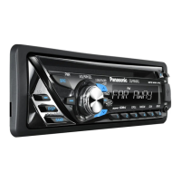
CQ-RD153N
 Loading...