Do you have a question about the Philips 22PFS5304/60 and is the answer not in the manual?
Details resolutions for PHx and PFx series TVs.
Lists ports and connections for various TV models.
Output power and audio features.
Aerial and satellite input details.
Supported USB file systems and playback formats.
Mains power specifications and operating temperature.
Safety regulations for repair and post-repair checks.
ESD precautions and handling sensitive components.
General notes, schematic conventions, spare parts, and BGA ICs.
Diagrams showing cable routing for 24" series TVs.
Diagrams showing cable routing for 32" and 43" series TVs.
Steps to remove the TV stand.
Instructions for removing the rear cover of 22"/24" series TVs.
Steps to remove the IR board for 22"/24" series TVs.
Procedure for removing the SSB and its connectors.
Overview of Service Alignment (SAM) and Factory modes.
Purpose and specifications of SAM for alignments and diagnostics.
Purpose and specifications for performing extended alignments.
Purpose and specifications of CSM for diagnostics.
Steps to update software using a .pkg file via USB.
Steps to update software using an .upg file via USB.
Purpose of error codes and the error buffer.
Methods for reading error codes via OSD or LED blinking.
Table of Layer 2 error codes and their associated devices.
High-level overview of the TV's main components and their connections.
Detailed information and pin description for the AD87010 IC.
Pin details for the TDSY-G430D IC.
Power Supply Unit circuit diagram for 24" 5603 series TVs.
System power schematic for the SSB.
LVDS connector pinout and panel power schematic.
HDMI 1, ARC, and CEC connections and circuitry.
HDMI 2 and CEC connections and circuitry.
Combined HDMI/MHL interface circuitry.
USB 2.0 interface schematic.
SPDIF optical output interface schematic.
SCART input connections and circuitry.
PC/DVI audio input connections.
RJ45 network connector schematic.
VGA input connections and circuitry.
T2 Tuner circuit for DVB-C/T/T2.
I2C control circuitry for the tuner.
Satellite digital interface circuitry.
LNB power supply circuitry.
ESD and surge protection circuitry.
Schematics for I2S and MIPS/UART/I2C/ICE interfaces.
Connections for audio output and phone jack.
NAND flash memory schematic.
NAND flash power supply schematic.
SPI NAND-MICRON flash schematic.
CI bus power control circuitry.
PCM signal routing and pin assignments.
PCMCIA power supply schematic.
Card detect circuitry.
Bluetooth function schematic for EMI solution.
UART and other signals for BUH daughter board.
Bathroom speaker audio output schematic.
System power schematic for the SSB.
LVDS connector pinout and panel power schematic.
HDMI 1, ARC, and CEC connections and circuitry.
HDMI 2 and CEC connections and circuitry.
Combined HDMI/MHL interface circuitry.
USB 2.0 interface schematic.
SPDIF optical output interface schematic.
RJ45 network connector schematic.
T2 Tuner circuit for DVB-C/T/T2.
I2C control circuitry for the tuner.
Satellite digital interface circuitry.
Schematics for I2S and MIPS/UART/I2C/ICE interfaces.
Connections for audio output and phone jack.
NAND flash memory schematic.
NAND flash power supply schematic.
SPI NAND-MICRON flash schematic.
CI bus power control circuitry.
PCM signal routing and pin assignments.
PCMCIA power supply schematic.
Card detect circuitry.
AC power supply schematic.
LED driver circuit schematic.
System power schematic for the SSB.
SPI NOR Flash and core power schematic.
Standby power supply schematic.
DDR3 power supply schematic.
Reset circuit schematic.
LVDS connector pinout and panel power schematic.
HDMI 1, ARC, and CEC connections and circuitry.
HDMI 2 and CEC connections and circuitry.
Combined HDMI/MHL interface circuitry.
USB 2.0 interface schematic.
SPDIF optical output interface schematic.
RJ45 network connector schematic.
T2 Tuner circuit for DVB-C/T/T2.
I2C control circuitry for the tuner.
Satellite digital interface circuitry.
LNB power supply circuitry.
ESD and surge protection circuitry.
Schematics for I2S and MIPS/UART/I2C/ICE interfaces.
Connections for audio output and phone jack.
NAND flash memory schematic.
NAND flash power supply schematic.
SPI NAND-MICRON flash schematic.
CI bus power control circuitry.
PCM signal routing and pin assignments.
PCMCIA power supply schematic.
Card detect circuitry.
IR LED circuit schematic.
IR receiver and standby LED circuitry.
IR receiver and standby LED circuitry.
Keyboard control panel and joystick circuit diagram.
Exploded view of 22"/24" series TV components.
Exploded view of 32" & 43" series TV components.
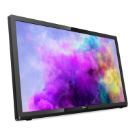
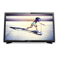
| Screen Size | 22 inches |
|---|---|
| Display Technology | LED |
| Smart TV | Yes |
| HDMI Ports | 2 |
| USB Ports | 1 |
| Audio Output | 10 W |
| Weight | 3.2 kg |
| Aspect ratio | 16:9 |
| VESA mounting | 100 x 100 mm |
| Operating System | SAPHI |
| Refresh Rate | 60 Hz |
| Resolution | 1920 x 1080 (Full HD) |
| Digital TV tuner | DVB-T/T2/C |




 Loading...