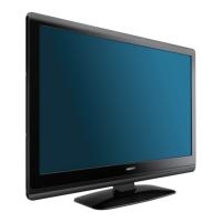
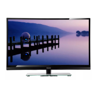
Do you have a question about the Philips 32PFL3904H/12 and is the answer not in the manual?
Provides detailed technical data and model information for the television sets.
Links to online product support, getting started guides, user manuals, FAQs, and software drivers.
Details side and back connector pinouts, including cinch, S-Video, headphone, and common interface.
Provides an overview of the chassis and references the block diagrams for PWB/CBA locations.
Outlines essential safety regulations for repair, including isolation transformer use and component replacement.
Highlights critical warnings regarding electrostatic discharge (ESD), high voltage sections, and component handling.
Offers general notes on measurements, schematic interpretations, spare parts, and BGA IC handling.
Lists and defines technical abbreviations used throughout the service manual for clarity.
Illustrates correct cable routing and management within the TV chassis for various models.
Describes recommended service positions using foam bars for easy access to internal components.
Details the step-by-step process for disassembling the TV, including rear cover, speakers, and panel removal.
Provides instructions for reassembling the TV set, emphasizing correct cable placement and EMC foam mounting.
Explains the use of test patterns via ComPair for determining defective parts in the TV.
Describes Service Default Mode (SDM) and Service Alignment Mode (SAM) for technical service operations.
Details a step-by-step start-up procedure to analyze errors in protection states and identify supply issues.
Introduces ComPair as a crucial hardware interface and software tool for diagnostics and upgrades.
Explains the error code buffer, types of errors (Layer 1 and Layer 2), and methods for reading and clearing them.
Describes the procedure for interpreting front LED blinking codes for Layer 1 and Layer 2 errors.
Details software and hardware protections, including supply errors and start-up monitoring mechanisms.
Offers practical tips for troubleshooting specific components like Ambilight, DC/DC converters, and loudspeakers.
Provides instructions for upgrading main and stand-by software via USB or other methods.
Outlines the required conditions for performing electrical adjustments and alignments, including power supply and test probes.
States that hardware alignments are not applicable for this specific chassis model.
Explains how to perform software alignments such as Tuner AGC and White Point adjustments.
Details how to set option codes for IC communication, model numbers, and feature activation.
Explains the process for resetting the NVM on a repaired SSB and setting the virgin bit.
Provides a comprehensive overview of the Service Alignment Mode (SAM) functions and submenus.
Introduces the Q543.1E LA chassis, its derivative status, and key components.
Describes the Integrated Power Board (IPB) and its specifications, including supply diversity.
Explains the DC-DC converters used in the chassis and their control mechanisms.
Details the key components of the front-end, including the tuner, IF demodulator, and AGC amplifier.
Explains the HDMI multiplexer implementation, EDID control, and differences from previous chassis.
Describes the PNX8543 as the main processor handling digital and analogue audio/video processing.
Explains the CI+ extension for Conditional Access systems and its copy protection capabilities.
Shows the internal block diagram and pin configuration for the NCP5422AD DC/DC converter.
Shows the internal block diagram and pin configuration for the ST1S10PH DC/DC converter.
Shows the internal block diagram and pin configuration for the LD3985M DC/DC converter.
Shows the internal block diagram and pin configuration for the DRX3926K front-end IC.
Shows the internal block diagram and pin configuration for the PNX8543 processor.
Shows the internal block diagram and pin configuration for the DP83816 Ethernet controller.
Shows the internal block diagram and pin configuration for the TPA3123D Class-D amplifier IC.
Illustrates the wiring connections for the 32" P&S models, showing power supply and SSB connections.
Illustrates the wiring connections for the 37" P&S models, showing power supply and SSB connections.
Illustrates the wiring connections for the 47" P&S models, showing power supply and SSB connections.
Illustrates the wiring connections for the 52" P&S models, showing power supply and SSB connections.
Shows the functional blocks and signal flow for the video processing section, including PNX8543.
Shows the functional blocks and signal flow for the audio processing section, including PNX8543.
Illustrates the control signals and clock distribution throughout the chassis, connecting various ICs.
Depicts the I2C communication paths between various components and the main processor.
Provides a high-level overview of the power supply lines distributed to different boards within the TV.
Presents the circuit diagram and PWB layout for the SSB v1 DC/DC +3V3/+1V2 power stage.
Presents the circuit diagram and PWB layout for the SSB v1 DC/DC +3V3/+1V2 stand-by power stage.
Shows the circuit diagram and PWB layout for the SSB v1 front-end tuner and demodulator section.
Details the circuit diagram and PWB layout for the SSB v1 PNX8543 processor power supply.
Shows the circuit diagram and PWB layout for the PNX8543 video stream and LVDS output.
Presents the circuit diagram and PWB layout for the PNX8543 audio amplifier section.
Details the circuit diagram and PWB layout for the PNX8543 audio subsystem.
Shows the circuit diagram and PWB layout for the PNX8543 analog AV inputs.
Presents the circuit diagram and PWB layout for the PNX8543 SDRAM interface.
Details the circuit diagram and PWB layout for the PNX8543 control, MIPS, Flash, and PCI interfaces.
Shows the circuit diagram and PWB layout for the PNX8543 stand-by control and debug functions.
Provides the circuit diagram and PWB layout for the SSB v1 bolt-on components.
Shows the circuit diagram and PWB layout for the SSB v1 analog IO and SCART connectors.
Presents the circuit diagram and PWB layout for the SSB v1 YPbPr, Side I/O, and S-video inputs.
Details the circuit diagram and PWB layout for the SSB v1 HDMI connectors and interface.
Shows the circuit diagram and PWB layout for the SSB v1 Ethernet interface.
Presents the circuit diagram and PWB layout for the SSB v1 PCMCIA interface.
Details the circuit diagram and PWB layout for the SSB v1 Class-D amplifier.
Shows the circuit diagram and PWB layout for the common display interface.
Presents the circuit diagram and PWB layout for the SSB v1 display power supply.
Shows the circuit diagram and PWB layout for the SSB v3 DC/DC +3V3/+1V2 power stage.
Presents the circuit diagram and PWB layout for the SSB v3 DC/DC +3V3-Stdby/+1V2-Stdby power stage.
Details the circuit diagram and PWB layout for the SSB v3 PNX8543 processor power supply.
Shows the circuit diagram and PWB layout for the PNX8543 video stream and LVDS output.
Presents the circuit diagram and PWB layout for the PNX8543 audio amplifier section.
Details the circuit diagram and PWB layout for the PNX8543 audio subsystem.
Shows the circuit diagram and PWB layout for the PNX8543 analog AV inputs.
Presents the circuit diagram and PWB layout for the PNX8543 SDRAM interface.
Details the circuit diagram and PWB layout for the PNX8543 control, MIPS, Flash, and PCI interfaces.
Shows the circuit diagram and PWB layout for the PNX8543 stand-by control and debug functions.
Provides the circuit diagram and PWB layout for the SSB v3 bolt-on components.
Shows the circuit diagram and PWB layout for the SSB v3 analog IO and SCART connectors.
Presents the circuit diagram and PWB layout for the SSB v3 YPbPr, Side I/O, and S-video inputs.
Details the circuit diagram and PWB layout for the SSB v3 HDMI connectors and interface.
Shows the circuit diagram and PWB layout for the SSB v3 Ethernet interface.
Presents the circuit diagram and PWB layout for the SSB v3 PCMCIA interface.
Details the circuit diagram and PWB layout for the SSB v3 Class-D amplifier.
Shows the circuit diagram and PWB layout for the common display interface.
Presents the circuit diagram and PWB layout for the SSB v3 display power supply.
Details the circuit diagram and PWB layout for the SSB v3 PNX5100 power supply.
Shows the circuit diagram and PWB layout for the PNX5100 control, PCI, and debug interfaces.
Presents the circuit diagram and PWB layout for the PNX5100 LVDS input/output.
Details the circuit diagram and PWB layout for the PNX5100 AmbiLight control.
Lists SRP signal references for various components on SSB v1, aiding in schematic navigation.
Lists SRP signal references for various components on SSB v1, aiding in schematic navigation.
Lists SRP signal references for various components on SSB v3, aiding in schematic navigation.
Lists SRP signal references for various components on SSB v3, aiding in schematic navigation.
| Screen Size | 32 inches |
|---|---|
| Resolution | 1366 x 768 pixels |
| Display Type | LCD |
| USB Ports | 1 |
| Audio Output | 2x5W |
| Smart TV | No |
| HD Type | HD Ready |
| Response Time | 5 ms |
| Contrast Ratio (Typical) | 1000:1 |
| Dynamic Contrast Ratio Marketing Name | Dynamic Contrast |
| Display Brightness | 300 cd/m² |
| Comb Filter | 3D |
| RMS Rated Power | 10 W |
| Number of Speakers | 2 |
| Component Video (YPbPr/YCbCr) In | 1 |
| SCART Ports Quantity | 1 |
| USB 2.0 Ports Quantity | 1 |
| Common Interface (CI) | Yes |
| Common Interface Plus (CI+) | No |
| Power Consumption (typical) | 45 W |
| Power Consumption (standby) | 0.5 W |
| Display Technology | LCD |
| Refresh Rate | 60 Hz |
| Viewing Angle, Horizontal | 176 degrees |
| Viewing Angle, Vertical | 176 degrees |
| Digital Signal Format System | DVB-T |
| Weight | 7.5 kg |
| Screen Format Adjustments | 16:9 |


