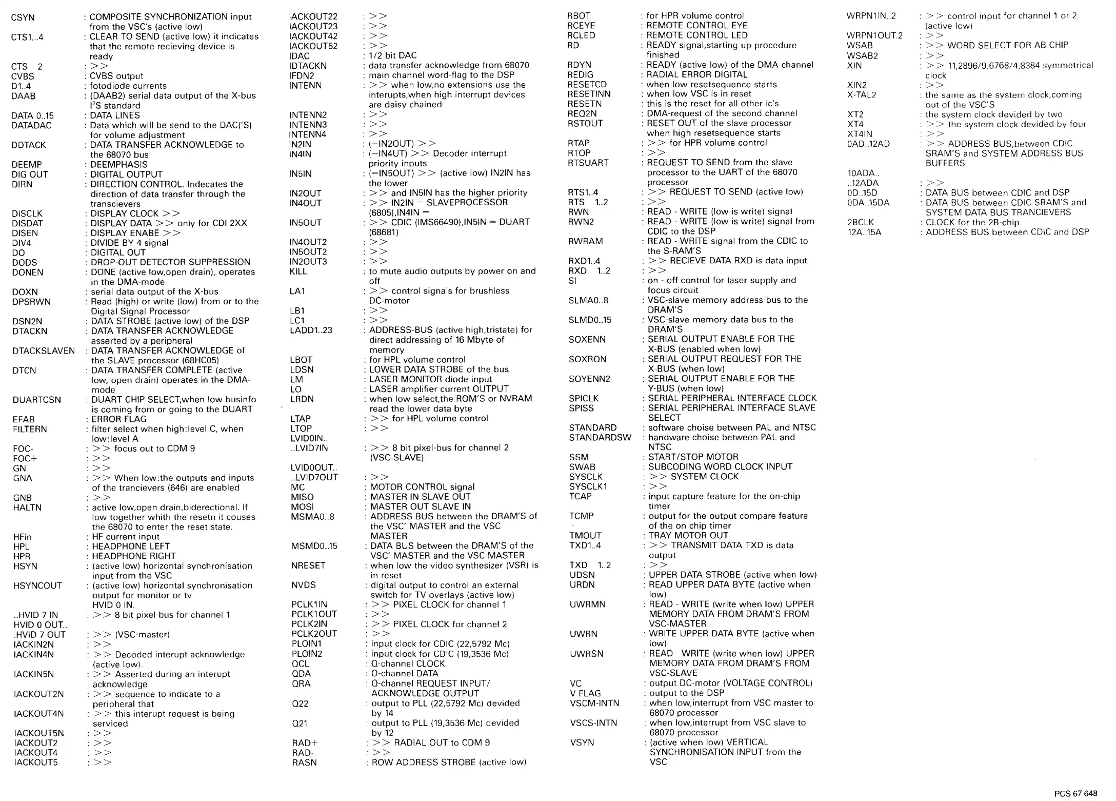
CSYN
: COMPOSITE SYNCHRONIZATION
input
IACKOUT22
:>>
RBOT
:
for
HPR
volume control
WRPN1IN
..
2
: > >
control
input
for channel 1 or 2
from
the VSC's (active low) IACKOUT23
:>>
RCEYE
: REMOTE CONTROL
EYE
(active low)
CTS1.
..
4
:
CLEAR
TO
SEND (active low) it indicates
IACKOUT42
:>>
RCLED
: REMOTE CONTROL
LED
WRPN1OUT.2
:>>
that the remote recieving device is IACKOUT52
:>>
RD
: READY signal.starting
up
procedure
WSAB
: > >
WORD SELECT
FOR
AB
CHIP
ready
IDAC
:
1/2
bit
DAC
finished
WSAB2
:>>
CTS
2
:>>
IDTACKN
: data transfer acknowledge from 68070
RDYN
: READY (active low)
of
the OMA channel
XIN
: > >
11,2896/9,6768/4,8384 symmetrical
CVBS
: CVBS
output
IFDN2
: main channel word-flag
to
the
DSP
REDIG
: RADIAL
ERROR
DIGITAL
clock
D1..4
:
fotodiode
currents INTENN
: > >
when
low.no extensions use the
RESETCD
:
when
low
resetsequence starts
XIN2
:>>
DAAB
: (DAAB2) serial data
output
of
the X-bus
interupts,when high interrupt devices
RESETINN :
when
low
VSC
is in reset
X-TAL2
: the same
as
the system clock.coming
I
2
S standard
are daisy chained
RESETN
: this is the reset for all other ic's
out
of
the VSC'S
DATA
0
..
15
:
DATA
LINES
INTENN2
:>>
RE02N : OMA-request
of
the second channel
XT2 : the system clock devided by two
DATADAC
: Data which will be send
to
the DAC('S)
INTENN3
:>>
RSTOUT
:
RESET
OUT
of
the slave processor
XT4
: > >
the system clock devided by four
for
volume
adjustment
INTENN4
:>>
when
high resetsequence starts
XT4IN
:>>
DDTACK
:
DATA
TRANSFER ACKNOWLEDGE to
IN21N
: (=IN2OUT)
> >
RTAP
: > >
for
HPR
volume control
0AD
..
12AD
: >
>
ADDRESS BUS,between
CDIC-
the 68070 bus
IN41N
: (=IN4UT)
> >
Decoder interrupt
RTOP
:>>
SRAM'S and SYSTEM ADDRESS BUS
DEEMP : DEEMPHASIS
priority
inputs RTSUART
: REQUEST
TO
SEND from the slave
BUFFERS
DIG
OUT
: DIGITAL OUTPUT
IN5IN
: (=IN5OUT)
> >
(active low)
IN21N
has
processor
to
the UART
of
the 68070
10ADA
..
DIRN
: DIRECTION CONTROL lndecates the
the
lower
processor
..
12ADA
:>>
direction
of
data transfer through the
IN2OUT
: > >
and IN5IN has the higher
priority
RTS1..4
: > >
REQUEST
TO
SEND (active
lowl
0D
..
15D
:
DATA
BUS between
CDIC
and
DSP
transcievers
IN4OUT
: > >
IN2IN = SLAVEPROCESSOR
RTS
1..2
:>>
0DA
..
15DA
:
DATA
BUS between CDIC-SRAM'S and
DISCLK : DISPLAY
CLOCK
> >
(6805),IN4IN
=
RWN
:
READ
- WRITE
(low
is write) signal
SYSTEM
DATA
BUS TRANCIEVERS
DISDAT
: DISPLAY
DATA
> >
only
for
CDI
2XX
IN5OUT
: > >
CDIC
(IMS66490),IN5IN =
DUART RWN2
: READ - WRITE (low is write) signal from
2BCLK
:
CLOCK
for the 2B-chip
DISEN
: DISPLAY ENABE
> >
(68681)
CDIC
to the
DSP
12A
..
15A
: ADDRESS BUS between
CDIC
and
DSP
DIV4 : DIVIDE
BY
4 signal
IN4OUT2
:>>
RWRAM
:
READ
- WRITE signal
from
the
CDIC
to
DO
: DIGITAL OUT
IN5OUT2
:>>
the S-RAM'S
DODS
: DROP-OUT
DETECTOR
SUPPRESSION IN2OUT3
:>>
RXD1..4
: > >
RECIEVE
DATA
RXD
is data
input
DONEN
:
DONE
(active low,open drain). operates
KILL
:
to
mute
audio
outputs
by
power
on and
RXD
1..2
:>>
in the DMA-mode
off
SI
: on -
off
control
for
laser supply and
DOXN
: serial data
output
of
the X-bus
LA1
: > >
control signals for brushless
focus circuit
DPSRWN
: Read (high) or
write
(low) from
or
to the DC-motor SLMA0
..
8
: VSC-slave
memory
address bus to the
Digital Signal Processor
LB1
:>>
DRAM'S
DSN2N
:
DATA
STROBE
(active low)
of
the
DSP
LC1
:>>
SLMD0
..
15
: VSC-slave
memory
data bus to the
DTACKN :
DATA
TRANSFER ACKNOWLEDGE
LADD1..23
: ADDRESS-BUS (active high,tristate) for
DRAM'S
asserted by a peripheral
direct addressing of
16
Mbyte
of
SOXENN
: SERIAL OUTPUT ENABLE
FOR
THE
DTACKSLAVEN
:
DATA
TRANSFER ACKNOWLEDGE
of
memory
X-BUS (enabled
when
low)
the SLAVE processor (68HC05)
LBOT : for
HPL
volume control SOXRQN
: SERIAL OUTPUT REQUEST
FOR
THE
DTCN
:
DATA
TRANSFER COMPLETE (active
LDSN
: LOWER
DATA
STROBE
of
the bus
X-BUS (when low)
low, open drain) operates in the OMA- LM
:
LASER
MONITOR diode input SOYENN2 : SERIAL OUTPUT ENABLE
FOR
THE
mode
LO
:
LASER
amplifier current OUTPUT
Y-BUS (when low)
DUARTCSN
: DUART
CHIP
SELECT.when
low
businfo
LRDN
:
when
low
select,the ROM'S
or
NVRAM
SPICLK
: SERIAL PERIPHERAL INTERFACE
CLOCK
is
coming
from
or
going to the DUART read the
lower
data byte
SPISS
: SERIAL PERIPHERAL
INTERFACE
SLAVE
EFAB
:
ERROR
FLAG
LTAP
: > >
for
HPL
volume control SELECT
FILTERN
: filter select
when
high:level
C,
when
LTOP
:>>
STANDARD
: software chaise between
PAL
and
NTSC
low:level A
LVIDOIN
..
STANDARDSW
: handware chaise between
PAL
and
FOC-
: > >
focus
out
to
COM
9
..
LVID71N
: > >
8
bit
pixel-bus for channel 2
NTSC
FOC+
:>>
(VSC-SLAVE)
SSM
: START /STOP MOTOR
GN
:>>
LVID0OUT..
SWAB
: SUBCODING WORD
CLOCK
INPUT
GNA
: > >
When
low:the
outputs and inputs
..
LVID7OUT
:>>
SYSCLK
: > >
SYSTEM
CLOCK
of
the trancievers (646) are enabled
MC
: MOTOR CONTROL signal
SYSCLK1
:>>
GNB
:>>
MISO
: MASTER
IN
SLAVE OUT
TCAP
: input capture feature for the on-chip
HALTN : active low.open drain,biderectional. If
MOSI
: MASTER OUT
SLAVE
IN
timer
low
together
whith
the resetn it causes
MSMA0
..
8
: ADDRESS BUS between the DRAM'S
of
TCMP
:
output
for
the
output
compare feature
the 68070
to
enter the reset state. the VSC' MASTER and the
VSC
of
the on chip
timer
HFin
:
HF
current input
MASTER
TMOUT : TRAY MOTOR OUT
HPL
: HEADPHONE
LEFT
MSMD0
..
15
:
DATA
BUS between the DRAM'S
of
the TXD1..4
: > >
TRANSMIT
DATA
TXD is data
HPR
: HEADPHONE
RIGHT
VSC' MASTER and the
VSC
MASTER
output
HSYN
: (active low) horizontal synchronisation NRESET :
when
low
the video synthesizer
(VSR)
is
TXD
1..2
:>>
input
from
the
VSC
in reset
UDSN
:
UPPER
DATA
STROBE
(active when low)
HSYNCOUT
: (active low) horizontal synchronisation
NVDS
: digital
output
to
control
an
external URDN :
READ
UPPER
DATA
BYTE
(active when
output
for
monitor
or tv
switch
for
TV overlays (active low) low)
HVID
0
IN.
PCLK1IN
:
>
>
PIXEL
CLOCK
for
channel 1
UWRMN
:
READ
- WRITE (write
when
low)
UPPER
..
HVID
7
IN
: > >
8
bit
pixel bus for channel 1
PCLK10UT
:>>
MEMORY
DATA
FROM
DRAM'S
FROM
HVID
0
OUT..
PCLK2IN
: > >
PIXEL
CLOCK
for
channel 2 VSC-MASTER
.HVID 7 OUT
: > >
(VSC-master)
PCLK2OUT
:>>
UWRN
:
WRITE
UPPER
DATA
BYTE
(active when
IACKIN2N
:>>
PLOIN1
: input clock for
COIC
(22,5792 Mc)
low)
IACKIN4N
: > >
Decoded interupt acknowledge
PLOIN2
:
input
clock for
CDIC
(19,3536 Mc)
UWRSN
:
READ
- WRITE (write
when
low)
UPPER
(active
low).
QCL
: Q-channel
CLOCK
MEMORY
DATA
FROM
DRAM'S
FROM
IACKIN5N
: > >
Asserted during
an
interupt
QDA : Q-channel
DATA
VSC-SLAVE
acknowledge
QRA
: Q-channel REQUEST INPUT/
vc
:
output
DC-motor
(VOLTAGE
CONTROL)
IACKOUT2N
: > >
sequence to indicate to a
ACKNOWLEDGE OUTPUT
V-FLAG
:
output
to
the
DSP
peripheral that
022
:
output
to
PLL
(22,5792 Mc) devided
VSCM-INTN :
when
low,interrupt from
VSC
master to
IACKOUT4N
: > >
this interupt request is being
by
14
68070 processor
serviced
Q21
:
output
to
PLL
(19,3536 Mc) devided
VS
CS-I
NTN :
when
low,interrupt from
VSC
slave to
1ACKOUT5N
:>>
by
12
68070 processor
IACKOUT2
:>>
RAD+
: > >
RADIAL OUT to
COM
9
VSYN
: (active
when
low) VERTICAL
IACKOUT4
:>>
RAD-
:>>
SYNCHRONISATION INPUT from the
IACKOUT5
:>>
RASN
:
ROW
ADDRESS
STROBE
(active low)
vsc
PCS
67
648


 To Next Page
 Loading...