EasyManua.ls Logo

Philips HTS3365/55 User Manual

Philips HTS3365/55
35 pages
To Next Page IconTo Next Page
Page #1 background imageLoading...
Page #1 background image
1 - 1
HTS3365/55
©
Copyright 2008 Philips Consumer Electronics B.V. Eindhoven, The Netherlands
All rights reserved. No part of this publication may be reproduced, stored in a retrieval system or
transmitted, in any form or by any means, electronic, mechanical, photocopying, or otherwise
without the prior permission of Philips.
Published b
y LM0835 Service Audio Printed in The Netherlands Subject to modification
DVD Home Theater System
Version 1.0
TABLE OF CONTENTS
Service Manual
Service
Tfswjdf
Tfswjdf
3139 785 34590
GB
Chapter
Location of PCB Boards .............................................. 1-2
Versions Variation....................................................... 1-2
Specifications .............................................................. 1-3
Measurement setups................................................... 1-4
Service Aids................................................................. 1-5
ESD & Safety instruction ............................................. 1-6
Lead-tree solding information...................................... 1-7
Setting procedure & Repair instructions......................... 2
Disassembly instruction & Service Postion....................3
Block & Wring Diagram .................................................. 4
VFD+JACK+VOL+STANDBY Board .............................. 5
Main Board ..................................................................... 6
Power Board................................................................... 7
AMP Board ..................................................................... 8
Mechanical Exploded View & Parts................................ 9
Revision List ................................................................. 10
Second Generation
This service manual is for HTS3365/55 Second Generation model,
which is different from the previous generation HTS3365/55 models.
For Second Generation model the serial number begin with
MF2AXXXXXXXXXX. Refer to the rating label illustration at right.
Question and Answer IconNeed help?

Do you have a question about the Philips HTS3365/55 and is the answer not in the manual?

Philips HTS3365/55 Specifications

General IconGeneral
BrandPhilips
ModelHTS3365/55
CategoryHome Theater System
LanguageEnglish

Summary

Location of PCB Boards

Version Variation

Service Scenario Matrix

Specifications

Measurement Setup

Service Aids

Service Tools

List of specialized tools for servicing the unit.

Compact Discs for Testing

Special discs for audio testing and burn-in.

Handling Chip Components

Guidelines for safely handling and mounting chip components.

ESD and Safety Precautions

ESD Protection Equipment

Equipment required for electrostatic discharge protection.

Laser Safety Warning

Warning about invisible laser radiation when the unit is open.

Lead-Free Solder Information

Identification of Lead-Free Solder

How to identify lead-free solder and related components.

Lead-Free Soldering Procedures

Rules and techniques for successful lead-free soldering.

System and Region Code Settings

System Reset Procedure

Steps to perform a system reset.

Region Code Change Procedure

Steps to change the DVD region code.

Software Upgrade Procedure

Guide for upgrading the system software.

Main Unit Repair Chart 1/3

Main Unit Repair Chart 2/3

Main Unit Repair Chart 3/3

Disassembly Instructions

Front Panel Assembly Disassembly

Steps to dismantle the front panel assembly.

AMP Board Disassembly

Steps to remove the AMP board.

Main Board Dismantling

Power Board Dismantling

VFD+JACK+VOL+STANDBY Board Dismantling

DVD Module Dismantling

Service Positions

Block Diagram

Wiring Diagram

Control Board

FTD Display Pin Assignment

Pin configuration for the Front Display Tube.

Control Board Circuit Diagram

Schematic diagram for the control board.

Control Board PCB Layout

Physical layout of components on the control board.

Circuit Diagram

PCB Layout - Top View

PCB Layout - Bottom View

Main Board

Main Board Internal IC Diagram

Internal circuitry diagram for the main IC.

Main Board Circuit Diagram

Schematic of the main board's electrical connections.

Main Board PCB Layout

Physical layout of components on the main board.

Power Board

Power Board Internal IC Diagram

Internal circuitry diagram for the power board's ICs.

Power Board Circuit Diagram

Schematic of the power board's electrical connections.

Power Board PCB Layout

Physical layout of components on the power board.

AMP Board

AMP Board Internal IC Diagram

Internal circuitry diagram for the amplifier's ICs.

AMP Board Circuit Diagram

Schematic of the amplifier board's electrical connections.

AMP Board PCB Layout

Physical layout of components on the amplifier board.
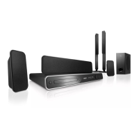
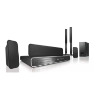
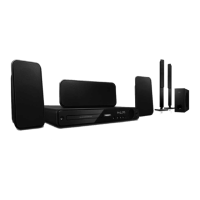
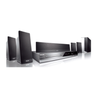
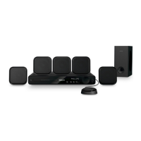
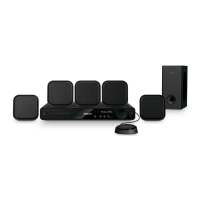
Mechanical Exploded View

Mechanical Part List

Revision List

Related product manuals