Circuit Descriptions, Abbreviation List, and IC Data Sheets
EN 90 LC7.2E LA9.
9.5.2 Supply
The internal voltages that are used are:
• 5 V (+5V_SW)
• 3.3 V (+3V3_MOJO)
• 1.2 V (+1V2_MOJO)
• 1.8 V (+1V8S_SW).
During start-up, it is important that the +1V8S_SW line comes
up earlier than the +3V3_MOJO line. In order to implement this,
a delay circuit is added which is shown in figure “Delay
circuitry”.
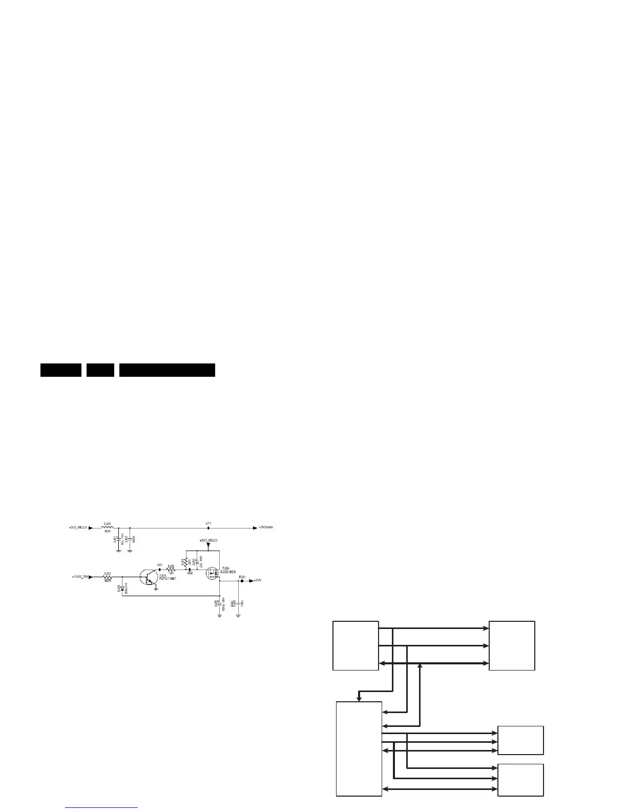
Figure 9-7 Delay circuitry
Item 7J05 switches the MOSFET “on” and “off” (item 7J04).
The diode (item 6J03) performs a short-circuit protection for the
+3V3 output stage.
9.6 Video Processing
The video processing is completely handled by the Trident SVP
CX32 video processor which features:
• CVBS-input for analogue signals.
• RGB-input for digital (DVB-T) signals.
• Motion and “edge-adaptive” de-interlacing.
• Integrated ADC.
• Built-in 8-bit LVDS transmitter.
• Colour stretch.
• Skin colour enhancement.
• 3D Digital Comb Video Decoder.
• Interlaced and Progressive Scan refresh.
• TeleText decoding.
• OSD and VBI/Closed Caption.
9.6.1 Video Application
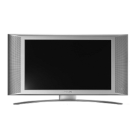
Figure 9-8 Block diagram video processing
“Block diagram video processing” shows the input and output
signals to and from the Trident Video Processor in EU
applications.
During analogue reception, a CVBS signal coming from the
analogue front-end is fed to the video processor via pin
CVBS1. During digital reception, the video signal coming from
the MPEG decoder (MOJO) is fed to the video processor via
pins FS1, PC_B, PC_G and PC_R.
The video processor also interfaces the SCART1 & 2 input,
side AV, EXT4 (HD where applicable) and HDMI1 & 2 input.
Through the SCART1 & 2 connectors, a monitor output is
foreseen.
9.7 Memory addressing
Figure “Memory block diagram” shows the interconnection
between the microprocessor, the FLASH memory, the Trident
Video Processor and the SDRAM.
Figure 9-9 Memory block diagram
Control signals CPU_RST, WR, RD and CE, address lines
A[0:19] and data lines D[0:7] are used for transferring data
between the microprocessor (item 7311) and the flash memory
(item 7310). Control signals CS, WR and RD, address lines
A[0:7] and data lines D[0:7] are used for transferring data
between the Trident Video Processor (item 7202) and the
microprocessor (item 7311). Control signals CX_BA0,
CX_BA1, CX_MCLK, CX_CLKE, CX_CS0, CX_RAS, CX_CAS
and CX_WE, address lines CX_MA[0:11] and data lines
DQ[0:15] are used for transferring data between the Trident
Video Processor and the SDRAM ICs (items 7204 and 7205).
G_16860_058.eps
310107
IB O _R _IN
Trident
Video Processor
SVP CX32
(DVB-T
demodu la to r
DigDŽ Front End
a nd decoder)
CVBS
S CART1
S C1_R_IN
S C1_CVBS _IN
S C1_FBL_IN
HD_Y_IN
S CART2
S IDE AV
FRONT_Y_CVBS _IN_T
S C2_Y_CVBS _IN
EXT4
HDMI
Decoder
HDMI1
HDMI2
HDMI_Y(0:7)
HDMI_Cb (0 :7)
HDMI_Cr(0:7)
On b o a rd E XT3
CVBS
SCART 1 Mon. out
PR_R2
PB_B2
Y_G2
S C1_G_IN
S C1_B_IN
PB_B3
FB1
IB O _G _IN
IB O _B _ IN
IB O _C V B S _IN
PC_R
PC_G
PC_B
F S 1
HD_PB_IN
HD_PR_IN
Y_G1
PB_B1
PR_R1
S C2_C_IN
FRONT_C_IN_T
Y_G3
C
PR_R3
F S 2
CVBS _OUT1
CVBS _OUT2
Ana lo g u e
Front End
CVBS _RF
CVBS 1
G_16860_060.eps
150307
SCART 2 Mon. out
7311
7202
7310
7204
7205
micro-
processor
1MB
Flash Memory
Trident CX
8MB
SDRAM
8MB
SDRAM
CPU_RST/WR/RD/CE
D[0:7]
A[0:19]
A[0:7]
D[0:7]
CS/WR/RD
CX_BA0/BA1/MCLK/
CLKE/CS0/RAS/CAS/WE
CX_MA[0:11]
DQ[0:15]
DQ[16:31]
CX_MA[0:11]
CX_BA0/BA1/MCLK/
CLKE/CS0/RAS/CAS/WE
Reneas
G_16860_062
220207