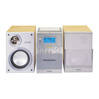
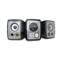
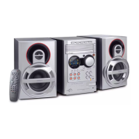
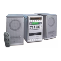
CONTROL BOARD
TABLE OF CONTENTS
IC Internal Block Diagram ..................................... 5-1to 5-4
Circuit Diagram ................................................................5-5
PCB Layout Top View ......................................................5-6
PCB Layout Bottom View ................................................5-7
Electrical Parts List ..........................................................5-8
5-1 5-1
MICROCONTROLLER AMPLIFIER
EM78P156EL
/RESET I * Input pin with Schmitt trigger. If this pin remains at logic low, the controller
will keep in reset condition.
P50~P53 I/O * P50~P53 are bi-directional I/O pins. P50 and P51 can also be defined as the
R-option pins. P50~P52 can be pulled down by software .
P60~P67 I/O * P60~P67 are bi-directional I/O pins. These can be pull-high or can be open-
drain by software programming. In addition, P60~P63 can be pull-down
also by software.
/INT I * External interrupt pin triggered by falling edge.
V
DD
-*Power supply.
V
SS
-*Ground.
Symbol I/O Function
OSCI I * XTAL type : Crystal input terminal or external clock input pin.
* ERC type: RC oscillator input pin.
OSCO I/O * XTAL type: Output terminal for crystal oscillator or external clock input pin.
* ERC type: Instruction clock ouput.
* External clock signal input.
TCC I * Real time clock/counter with Schmitt trigger input pin, must be tied to V
DD
or V
SS
if not in use.
PIN DESCRIPTION
FUNCTIONAL BLOCK DIAGRAM
WDT Timer
IOC5
R5
Instruction
Decoder
ROM
Interrupt
Controller
R1(TCC)
Oscillator/Timing
Control
Prescaler
RAM
R4
Instruction
register
R2
Stack
OSCI OSCO /RESET
DATA & CONTROL BUS
TCC
/INT
ACC
R3
ALU
WDT
Time-out
IOCA
Sleep
& Wake
Control
P
5
0
P
5
2
P
5
3
P
5
1
IOC6
R6
P
6
0
P
6
2
P
6
3
P
6
1
P
6
4
P
6
6
P
6
7
P
6
5
 Loading...