7.
Circuit description
TIMING CIRCUIT, UNIT PM
5715-1
Refer to the circuit diagram Fig.
12
—
2 or
Fig.
12-4.
Oscillator,
Schmitt trigger and
gating
circuits
The oscillator consists mainly of
transistors
TS103,
105,
108 and
109.
Its repetition
frequency is determined
by capacitor network
Cl
05,
C107...113, which are
connected to the
oscillator with front
panel switch
SKI,
REPETITION
TIME. Continuous
setting of the
frequency is
achieved with constant current
generator TS104, TS107,
TS106 and TS109,
which
is operated with front panel control VER-
NIER,
R1.
The output of
the oscillator is connected
to
in-
put terminal 10 of
OR/ NOR gate
IC101,
whose
second input
terminal
9
must be low
to
enable
the signal
to pass through (Fig. 7
—
1).
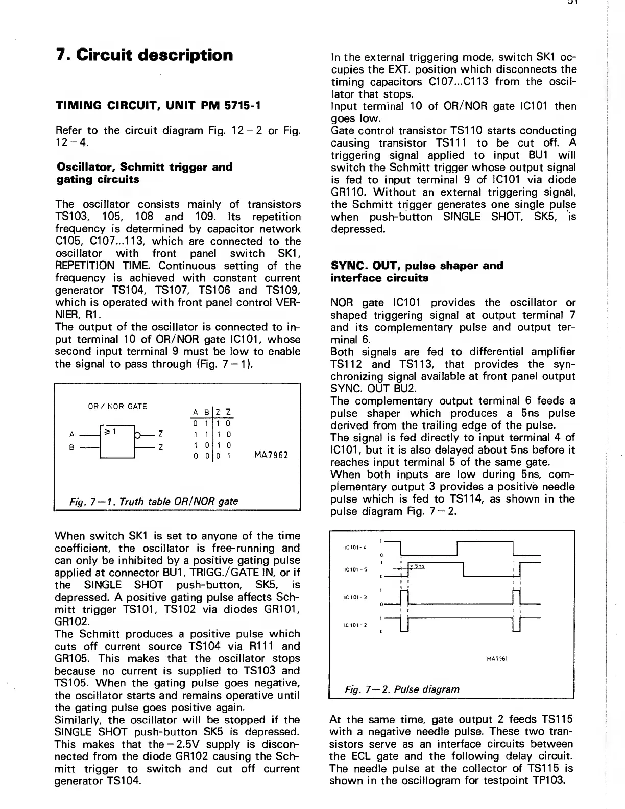
OR/ NOR GATE
(D
< z z
0
1 1
0
1
1
1
0
1
0
1
0
oo 0
1
MA7962
Fig.
7—1.
Truth
table
OR
I
NOR
gate
In
the
external triggering mode, switch
SKI
oc-
cupies the
EXT. position which disconnects the
timing capacitors
Cl
07. ..Cl 13 from the oscil-
lator that
stops.
Input terminal
10
of
OR/NOR
gate
IC101
then
goes low.
Gate control transistor
TS110 starts conducting
causing transistor TS1
11
to be cut
off. A
triggering signal applied to input
BUI
will
switch the
Schmitt trigger whose output signal
is fed to input
terminal 9 of
IC101
via diode
GR110. Without an
external triggering signal,
the Schmitt trigger generates one single
pulse
when
push-button
SINGLE
SHOT,
SK5, is
depressed.
SYNC. OUT, pulse
shaper and
interface circuits
NOR gate
IC101 provides the oscillator or
shaped triggering
signal
at
output terminal
7
and its complementary pulse
and output ter-
minal
6.
Both signals are fed to
differential amplifier
TS1
1
2
and TS1
1
3,
that
provides the syn-
chronizing
signal available at front
panel
output
SYNC.
OUT
BU2.
The complementary output terminal
6
feeds a
pulse shaper
which produces a 5ns pulse
derived from
the
trailing edge of the pulse.
The signal is fed directly to input terminal
4
of
IC101, but it is also delayed about 5ns before it
reaches input terminal 5 of the same gate.
When
both
inputs are low during 5ns, com-
plementary output
3
provides a positive needle
pulse
which is fed to TS114, as shown in the
pulse
diagram
Fig.
7-2.
When switch
SKI
is set to anyone
of
the
time
coefficient, the oscillator
is free-running and
can only be
inhibited by
a
positive
gating
pulse
applied at connector
BUI,
TRIGG./GATE
IN,
or if
the
SINGLE
SHOT
push-button, SK5, is
depressed. A positive gating
pulse affects Sch-
mitt trigger TS101,
TS102 via diodes GR101,
GR102.
The Schmitt produces a
positive pulse which
cuts
off current source
TS104
via
R111 and
GR105. This makes that the
oscillator stops
because no
current is
supplied
to
TS103 and
TS105. When the gating pulse goes
negative,
the
oscillator starts and remains
operative until
the
gating pulse goes positive
again.
Similarly, the oscillator
will be
stopped
if the
SINGLE SHOT
push-button SK5 is depressed.
This makes that the
-2.5V supply is discon-
nected
from the diode GR102 causing the Sch-
mitt trigger
to
switch and cut
off current
generator TS1
04.
MA7S61
Fig.
7—2.
Pulse
diagram
At
the same
time, gate
output
2
feeds TS115
with
a
negative needle
pulse. These two tran-
sistors serve as an
interface circuits between
the
ECL gate and the
following delay circuit.
The needle pulse at the
collector of TS115 is
shown in the oscillogram
for testpoint
TP103.
 Loading...