Delay
circuit
The
5ns pulse from
interface transistor TS115
controls
the delay circuit, consisting
of dif-
ferential
stage TS116, TS117,
emitter follower
TS119,
timing capacitors Cl 23. ..Cl
30,
switch
diode
GR112, and constant current
generator
TS118.
The
positive pulse is
applied
to
the
base
of
TS1 1
6 which cuts off TS1
1
7.
The
negative step
at the emitter of TS1
1 9 is
coupled through
the timing capacitor
selected
and keeps TS117
in the
non-conductive state
and cuts
off diode GR112.
The current
generated by TS118
is set with
VERNIER
control R2 and
will now charge
capacitors
Cl 23
and one of capacitors
Cl 24. ..Cl 30
as set
with the
DELAY
switch SK2.
When
the charging
level has reached zero,
TS117
and GR112
start conducting and TS116
cuts off. The timing
capacitors will
now
discharge through
GR112. At the collector
of
TS117
a
pulse occurs,
whose duration is
deter-
mined by
the selected value of the timing
capacitors (DELAY
switch) and the value of
the
charging current (VERNIER
control). This pulse
is shown in
the oscillogram recorded
at test
point
TP104.
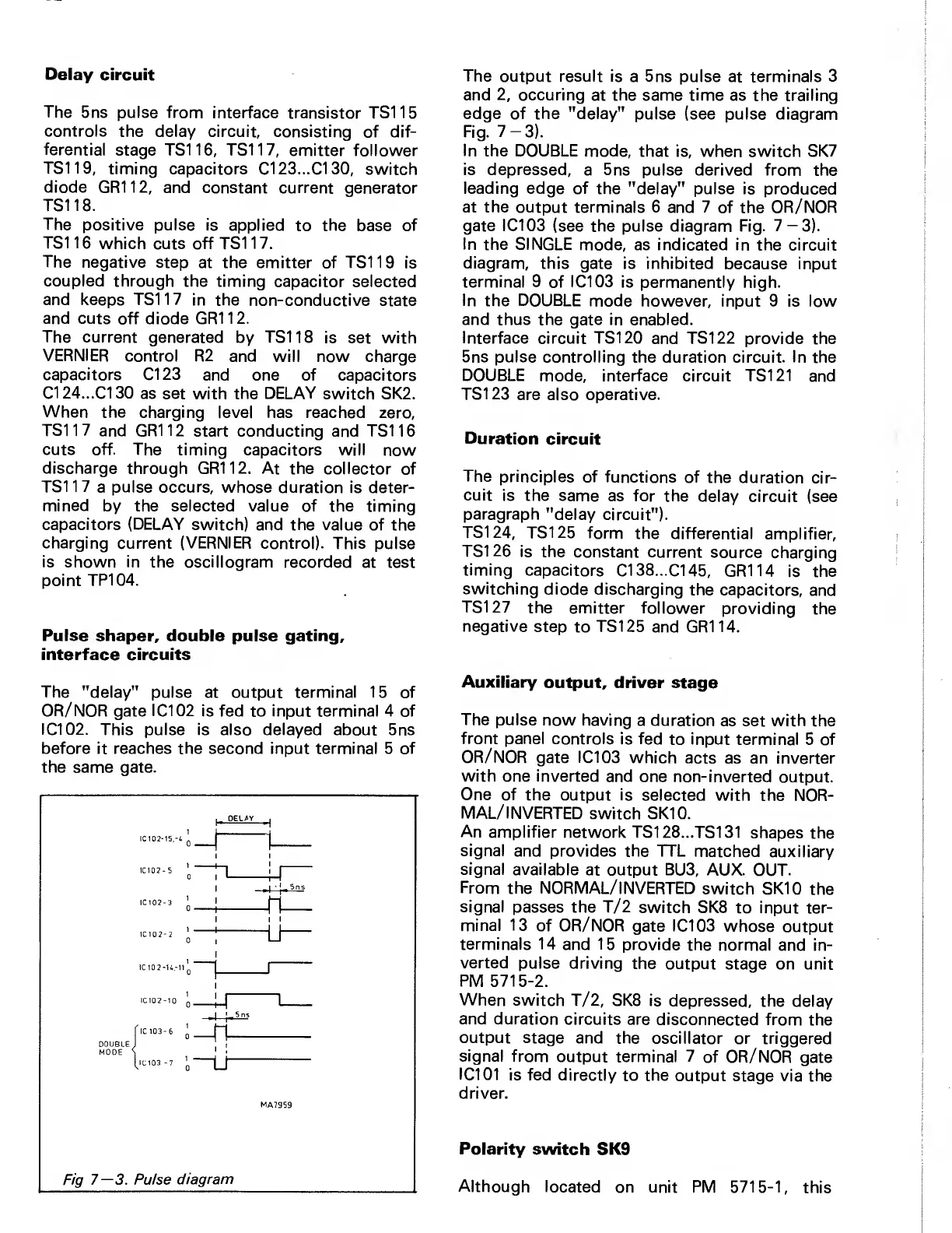
Pulse shaper, double pulse gating,
interface circuits
The
"delay" pulse at output terminal 15 of
OR/NOR gate 1C102 is fed to input terminal 4 of
IC102.
This pulse is also delayed about 5ns
before it reaches the second input terminal 5 of
the same gate.
DOUBLE
MODE
T
-Tl-
I
I
-Lh
j
;
(_r
MA7959
Fig
7—3.
Pulse
diagram
The
output result is
a 5ns pulse at terminals
3
and
2,
occuring
at the same
time
as the trailing
edge of the "delay"
pulse (see pulse diagram
Fig.
7-3).
In
the DOUBLE mode,
that is, when switch SK7
is depressed,
a 5ns pulse derived from
the
leading edge of
the "delay" pulse is produced
at the output terminals 6
and 7 of
the
OR/NOR
gate IC103
(see the pulse diagram Fig.
7
—
3).
In
the SINGLE
mode, as indicated in
the circuit
diagram,
this gate is inhibited
because input
terminal
9 of
IC103
is permanently
high.
In
the
DOUBLE
mode
however, input 9 is low
and thus
the
gate in enabled.
Interface circuit TS120
and
TS122
provide the
5ns pulse controlling
the duration circuit.
In
the
DOUBLE
mode,
interface
circuit TS121 and
TS123
are also operative.
Duration
circuit
The principles
of
functions of
the duration
cir-
cuit
is the same
as for
the delay circuit
(see
paragraph
"delay
circuit").
TS124,
TS125 form
the differential
amplifier,
TS126
is the
constant current
source
charging
timing capacitors
Cl
38.
..Cl
45,
GR114 is
the
switching
diode discharging
the
capacitors,
and
TS127
the emitter
follower
providing
the
negative
step
to
TS125
and GR114.
Auxiliary
output, driver stage
The pulse
now having
a duration
as set with
the
front
panel controls is fed
to
input
terminal 5 of
OR/NOR
gate
IC103
which acts
as an inverter
with
one inverted and
one non-inverted
output.
One of
the output is selected
with
the NOR-
MAL/INVERTED
switch SK10.
An
amplifier
network TS128...TS131
shapes
the
signal and
provides the TTL
matched
auxiliary
signal available
at output BU3,
AUX.
OUT.
From
the
NORMAL/
INVERTED
switch SK10
the
signal
passes the T/2
switch SK8
to input ter-
minal 13
of OR/NOR
gate
IC103
whose
output
terminals 14
and
15
provide
the normal
and in-
verted pulse
driving
the output
stage on unit
PM
5715-2.
When
switch
T/2, SK8 is
depressed,
the delay
and duration
circuits are
disconnected from
the
output stage
and the
oscillator or triggered
signal
from
output terminal 7
of OR/NOR
gate
IC101
is fed directly
to the
output stage via
the
driver.
Polarity
switch SK9
Although located
on unit PM 5715-1,
this
 Loading...