switch
controls
the output
amplifiers
on unit
PM
5715-2.
Refer
to paragraph
"Positive
and
negative
pulse
amplifiers".
OUTPUT
CIRCUIT: PM
5715-2
Refer
to the circuit
diagram Fig. 12
—
6 or
Fig.
12
-
8
.
The current
path
is
now diverted through
TS203
and TS206.
The
charged capacitors
will discharge through
TS206.
The discharging time
is set with
SK4
and ver-
nier
tf, R5, that controls the current through
TS206. When
the voltage has dropped
to
—
0.7V,
diode GR202 will turn on and
clamp the
voltage.
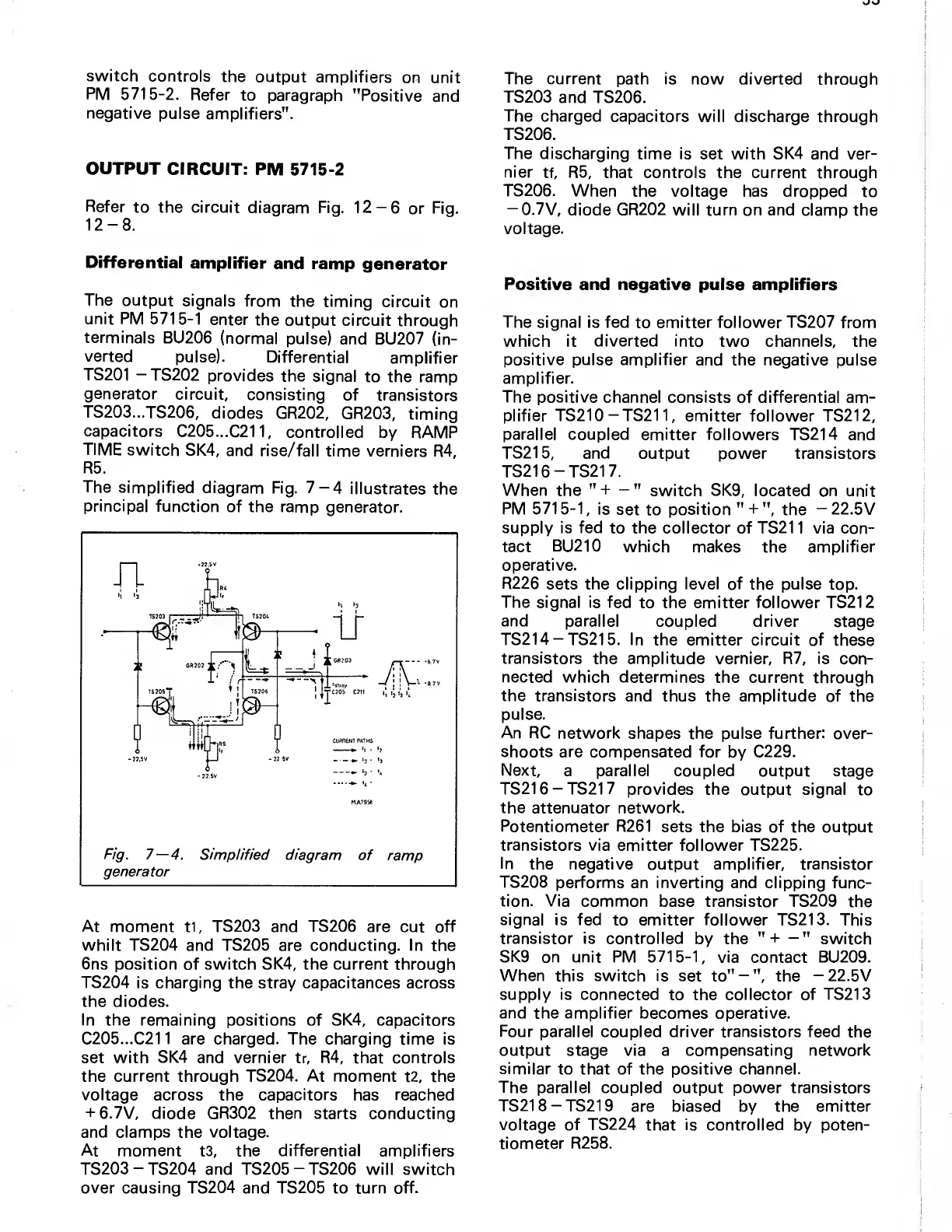
Differential
amplifier
and ramp
generator
The
output signals
from
the timing
circuit
on
unit PM
5715-1
enter
the output
circuit
through
terminals
BU206
(normal
pulse)
and BU207
(in-
verted
pulse).
Differential
amplifier
TS201
—
TS202
provides
the signal
to the ramp
generator
circuit,
consisting
of
transistors
TS203...TS206,
diodes
GR202,
GR203,
timing
capacitors
C205...C211,
controlled
by RAMP
TIME
switch
SK4,
and rise/fall
time verniers
R4,
R5.
The
simplified
diagram Fig.
7-4
illustrates
the
principal
function of
the ramp
generator.
At
moment
ti, TS203
and
TS206
are cut off
whilt TS204 and TS205
are conducting.
In
the
6ns position of switch
SK4,
the current through
TS204
is charging the stray capacitances across
the diodes.
In the
remaining positions of
SK4,
capacitors
C205...C211 are charged. The charging time is
set with
SK4
and vernier tr, R4, that controls
the
current
through
TS204. At
moment
t2,
the
voltage across
the
capacitors
has
reached
+
6.7V, diode GR302 then starts
conducting
and clamps
the
voltage.
At moment
t3,
the differential amplifiers
TS203-TS204 and TS205-TS206 will switch
over
causing TS204 and TS205 to turn off.
Positive
and negative pulse amplifiers
The
signal is fed
to
emitter follower TS207
from
which
it
diverted into
two channels, the
positive pulse amplifier
and the negative pulse
amplifier.
The positive
channel consists of differential am-
plifier TS210-TS211,
emitter follower TS212,
parallel coupled emitter followers
TS214 and
TS215, and
output power transistors
TS216-TS217.
When the
"+
-"
switch
SK9,
located on unit
PM 5715-1,
is
set
to
position
"
+
",
the -22.5V
supply is fed
to the collector
of
TS21 1 via con-
tact
BU210
which makes
the
amplifier
operative.
R226 sets
the clipping
level
of the
pulse
top.
The signal is fed
to the emitter follower TS212
and parallel
coupled driver stage
TS214-TS215. In
the emitter circuit of
these
transistors
the
amplitude
vernier, R7, is
con-
nected which determines
the current through
the transistors
and thus the amplitude of
the
pulse.
An RC network
shapes the pulse further: over-
shoots are
compensated
for
by C229.
Next,
a parallel coupled output stage
TS216-TS217
provides the output signal
to
the attenuator network.
Potentiometer R261
sets the bias of the output
transistors via
emitter follower TS225.
In
the negative output amplifier, transistor
TS208 performs
an inverting and clipping func-
tion. Via
common base transistor TS209
the
signal is fed
to
emitter follower
TS213. This
transistor is controlled
by the
"+
-"
switch
SK9
on unit PM
5715-1,
via
contact
BU209.
When this switch is set
to"
—
",
the
—22.5V
supply is connected
to the
collector of TS213
and the amplifier becomes operative.
Four
parallel coupled driver transistors feed
the
output stage via a compensating network
similar
to that of the positive channel.
The
parallel coupled output power transistors
TS218-TS219
are biased by the emitter
voltage of TS224
that
is controlled
by poten-
tiometer R258.
 Loading...