Do you have a question about the Pioneer VSX-1020-K and is the answer not in the manual?
General safety precautions for customer and technician protection during servicing.
Importance of using specified replacement parts with special safety characteristics.
Conformance to product regulations and maintaining a safe servicing environment.
Procedures for optimum product adjustments and confirmation of characteristics within specifications.
Guidelines for using specified substances and amounts for lubricants, glues, and replacement parts.
Proper cleaning procedures for optical pickups, tape heads, and projection monitor lenses.
Setting shipping mode or installing shipping screws to protect products during transit.
Guidelines for using lead-free solder and appropriate soldering iron specifications for repairs.
Notes on difficulty of replacing discrete parts, recommending Assy replacement.
Safety cautions regarding discharging and ground point connections before servicing.
Detailed technical specifications including power output, audio, tuner, video, and digital input sections.
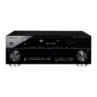
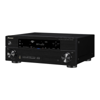
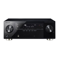
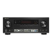
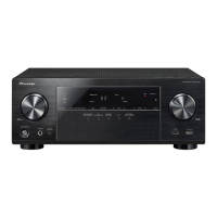
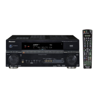
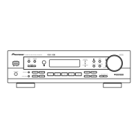
Identification and description of controls and indicators on the front panel.
Explains the meaning of indicator lights on the display for signal status and modes.
Explains how to operate the receiver using the remote control, detailing function buttons and source selection.
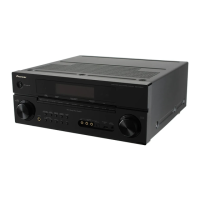
Illustrates and describes the various input/output terminals located on the rear of the unit.
Recommended checks to ensure product quality and functionality after service procedures are completed.
Visual identification and labeling of various Printed Circuit Boards (PCBs) within the unit.
Lists required jigs and their part numbers for diagnosis and service procedures.
Lists specified lubricants and glues with their part numbers and application notes.
Shows the overall wiring connections between major assemblies and components of the unit.
Illustrates the signal flow and processing for digital audio within the D-MAIN Assy.
Illustrates the signal flow and processing for analog audio within the AUDIO Assy.
Shows the signal flow and processing for digital video signals within the D-MAIN Assy.
Illustrates the signal flow and processing for analog video signals within the COMPONENT Assy.
Illustrates the ground connections and distribution across various assemblies.
Step-by-step troubleshooting guide for identifying and resolving audio and operational issues.
Details error codes, detection methods, and descriptions for abnormalities in the amplifier system.
Instructions on how to enter the release mode for specific error conditions.
Checks related to power supply voltages for various ICs involved in HDMI and DVC functions.
Troubleshooting steps for crystal oscillator circuits.
Troubleshooting steps for reset signal paths and circuits.
Troubleshooting steps for HDMI input and output signals.
Checks for proper signal output and connections related to HDMI input ports 1 through 4.
Troubleshooting steps for the BD IN signal path.
Troubleshooting steps for the front HDMI input signal.
Troubleshooting steps for Component IN signals.
Checks for signal output from HDMI OUT terminals when operating above 480p resolution.
Troubleshooting steps for Component IN and HDMI OUT at 480i resolution.
Checks related to the HDMI output signal path and indicators.
Troubleshooting steps for Composite IN and HDMI OUT signals.
Troubleshooting steps for Component IN signals, including Composite S OUT considerations.
Troubleshooting steps for S-Video input and output signals.
Troubleshooting steps for Composite IN and OUT signals when DVC is ON.
Procedures for updating GUI/JPEG via USB, focusing on Composite/S/Component OUT.
Procedures for updating GUI/JPEG via USB, focusing on HDMI OUT.
Visual guide to component locations and test points on the D-MAIN Assy for diagnosis.
Details error codes, detection methods, and descriptions for abnormalities in the amplifier system.
Instructions on how to enter the release mode for specific error conditions.
Explanation of the TEST MODE, its purposes, basic operations, and how to reset error counts.
Describes the CEC TEST function for verifying HDMI output terminal operation.
Procedure for safely discharging capacitors in the MAIN Assy before servicing.
Important points to be grounded when the rear panel is removed to prevent short circuits.
Identifies specific screws used for the chassis back panel.
Step-by-step instructions for disassembling the front panel and D-MAIN Assy.
Procedure for removing the heatsink section, cautioning about its heat.
Instructions for removing the AUDIO and COMPOSITE Assys, including reassembly notes.
Detailed steps for disassembling and reassembling the MAIN Assy, including chassis back and D-MAIN Assy removal.
Step-by-step guide for updating the unit's firmware using a USB memory device.
Procedure for adjusting idle current, including measurement points and VR settings.
Illustrates the packing configuration of the unit and its accessories for shipping.
Exploded views showing the exterior parts and their assembly order.
Comprehensive list of all exterior parts, their mark numbers, descriptions, and part numbers.
Highlights differences in specific parts between VSX-1020-K and VSX-1025-K models.
Schematic diagram for the AUDIO Assy, detailing its internal circuitry and connections.
Schematic diagram for the COMPONENT Assy, showing its circuit layout.
Schematic diagrams for COMPOSITE, MIC, F-VIDEO, and BRIDGE2 Assys.
Schematic diagrams for F-HDMI, USB MTG, and HDMI MTG Assys.
Schematic diagram for the AMP Assy, showing the amplifier circuits for various channels.
Schematic diagrams for DISPLAY, HEADPHONE, and POWER SW Assys.
Schematic diagram for the first part of the D-MAIN Assy.
Schematic diagram for the second part of the D-MAIN Assy.
Schematic diagram for the third part of the D-MAIN Assy.
Schematic diagram for the fourth part of the D-MAIN Assy.
Schematic diagram for the fifth part of the D-MAIN Assy, focusing on HDMI parts.
Schematic diagram for the sixth part of the D-MAIN Assy, detailing the video scalar.
Schematic diagram for the seventh part of the D-MAIN Assy, focusing on digital audio interfaces.
Schematic diagram for the eighth part of the D-MAIN Assy, showing SDRAM and Flash ROM connections.
Schematic diagram for the ninth part of the D-MAIN Assy, detailing DSP connections and oscillators.
Schematic diagram for the tenth part of the D-MAIN Assy, showing DACs and regulators.
Schematic diagram for the eleventh part of the D-MAIN Assy, detailing DAC circuits.
Schematic diagram for the twelfth part of the D-MAIN Assy, focusing on power supply circuits.
Schematic diagrams for the MAIN and BRIDGE1 Assys.
PCB layout showing component placement and connector pin assignments for the AUDIO Assy.
PCB layout showing component placement and connector pin assignments for the COMPONENT Assy.
PCB layouts for COMPOSITE, MIC, F-VIDEO, and BRIDGE2 Assys.
PCB layouts for F-HDMI, USB MTG, and HDMI MTG Assys.
PCB layout showing component placement and connector pin assignments for the AMP Assy.
PCB layouts for DISPLAY, HEADPHONE, and POWER SW Assys.
PCB layout showing component placement and connector pin assignments for the D-MAIN Assy.
PCB layout showing component placement and connector pin assignments for the MAIN Assy.
PCB layouts for BRIDGE1, GUIDE3, GUIDE-L, and GUIDE-R Assys.
List of all major assemblies with their part numbers.
Parts list for semiconductors on the AUDIO Assy.
Parts list for semiconductors on the COMPONENT Assy.
Parts list for semiconductors on the COMPOSITE Assy.
Parts list for semiconductors on the MIC Assy.
Parts list for semiconductors on the F-VIDEO Assy.
Miscellaneous parts list for the BRIDGE2 Assy.
Parts list for semiconductors on the DISPLAY Assy.
Parts list for semiconductors on the HEADPHONE Assy.
Miscellaneous parts list for the POWER SW Assy.
Parts list for semiconductors on the D-MAIN Assy.
Parts list for semiconductors on the MAIN Assy.
Parts information for the BRIDGE1 Assy.
Parts information for the GUIDE3 Assy.
Parts information for the GUIDE-L Assy.
Parts information for the GUIDE-R Assy.
| power requirements | AC 120 V/60 Hz |
|---|---|
| power consumption | 245 Watts |
| standby power consumption | Less than 0.5 Watts |
| width | 16.55 inches |
|---|---|
| height | 6.23 inches |
| depth | 14.93 inches |
| weight | 22.4 lbs |