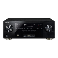
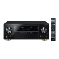
Do you have a question about the Pioneer VSX-920-K and is the answer not in the manual?
Lists essential jigs required for performing diagnostics and service operations.
Illustrates the complete wiring interconnections between major assemblies and components.
Presents a high-level functional overview of the unit's internal architecture.
Provides step-by-step diagnostic procedures to identify and resolve faults, starting with DSP issues.
Offers simple diagnostic steps for common HDMI display and sound problems.
Detailed troubleshooting steps and procedures for addressing HDMI connection and authentication issues.
Provides detailed steps and illustrations for disassembling the unit, focusing on cable dressing.
Details the procedure for adjusting the idle current on the amplifier board for optimal performance.
Presents the detailed schematic for the input assembly, showing component connections and signal paths.
Provides the schematic diagram for the amplifier assembly, detailing audio output stages.
Includes schematics for speaker, headphone, and microphone interface circuits.
Displays schematics for various interface boards including PT, HP_GUIDE, CNT1, CNT2, and GUIDE assemblies.
Presents the schematic for the video processing circuitry, handling input and output signals.
Provides schematics for front panel, F-VIDEO, and function control assemblies.
Contains schematics for the main control board and voltage regulator assemblies.
Displays the first part of the HDMI assembly schematic, detailing interface circuitry.
Presents the second part of the HDMI assembly schematic, completing the interface circuit details.
Shows the first part of the DSP assembly schematic, detailing digital signal processing components.
Provides the second part of the DSP assembly schematic, completing the digital processing circuit.
Displays the schematic for the USB interface assembly, including control and data transfer circuitry.
Illustrates the component placement and connection points for the Input Assy PCB.
Shows the PCB layout for speaker, headphone, and microphone interface assemblies.
Displays PCB layout diagrams for PT, HP_GUIDE, CNT1, CNT2, GUIDE_L, and GUIDE_R assemblies.
Illustrates the PCB layout for the video assembly, showing component placement.
Shows the PCB layout for the main control and voltage regulator assemblies.
Displays the first part of the HDMI assembly PCB layout, showing component placement.
Presents the second part of the HDMI assembly PCB layout, completing the interface board diagram.
Shows the PCB layout for the DSP assembly, detailing component placement and connections.
Displays the PCB layout for the USB assembly, showing component placement.
| power requirements | AC 120 V/60 Hz |
|---|---|
| power consumption | 270 Watts |
| standby power consumption | Less than 0.4 Watts |
| width | 16.55 inches |
|---|---|
| height | 6.23 inches |
| depth | 13.71 inches |
| weight | 21.3 lbs |