Do you have a question about the Pioneer XW-NAC3-R and is the answer not in the manual?
| Type | Wireless Speaker System |
|---|---|
| Color Options | Red (XW-NAC3-R) |
| Connectivity | Wi-Fi, Bluetooth, USB |
| Supported Audio Formats | MP3, WMA |
| Inputs | USB, AUX |
| Compatibility | iOS, Android, Windows |
Identifies the product type and compatible devices.
Specifies the order number for the manual.
Details applicable models and types, including power requirements and remarks.
Clarifies the manual is for qualified service technicians, not DIY users.
Warns about explosion danger and proper handling/disposal of lithium batteries.
Covers using specified parts, avoiding modifications, and proper soldering.
Details on maintaining original performance through adjustments.
Guidance on using specified lubricants and adhesives.
Instructions and precautions for using lead-free solder and appropriate soldering irons.
Detailed technical specifications for the amplifier, speaker, network, and miscellaneous sections.
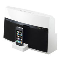
Explains "Made for iPod" and "Works with iPhone" certifications.
Instructions on battery installation and replacement for the remote control.
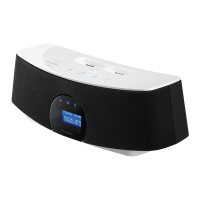
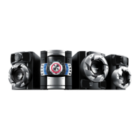
Identifies and describes the functions of buttons and indicators on the front/top panel.
Details how to select input sources for iPod, Bluetooth, etc.
Information on the USB terminal and the importance of using the cover.
Critical warning about storing the USB terminal cover away from children.
Explains the function of various playback control buttons on the remote.
Describes how to select albums for playback on iPod/iPhone.
Explains how to switch track information display during playback.
Instructions for adjusting the listening volume.
Lists crucial checks to perform after servicing to ensure product quality and customer satisfaction.
Details specific checks for video image quality and audio performance.
Provides a list of major assemblies with their corresponding part numbers.
Important notes regarding unavailable parts (NSP) and safety markings.
Lists required jigs for diagnosis and software updates, with part numbers and purpose.
Shows the complete wiring connections between different PCB assemblies.
Provides a high-level overview of the system's functional blocks and their interconnections.
Details the internal components and connections of the Dock PCB Assembly.
Outlines the circuit diagram for the Bluetooth PCB Assembly.
Shows the schematic for the main PCB, including various ICs and connections.
Illustrates the PCB layout and connections for the Display Assembly.
Step-by-step troubleshooting flowchart for "No power" issues.
Specific voltage checks to diagnose power-related problems.
Procedure to check for activated protection circuits during diagnosis.
Explains the network function constitution and provides a diagnostic flow chart.
A visual guide to troubleshoot network connection issues.
Troubleshooting steps for USB connection issues, including file system and format checks.
Steps to troubleshoot Internet Radio connectivity problems.
Initial connection checks for various ICs and power supply points.
Detailed checks for 5V and 3.3V power supplies to different ICs.
Step-by-step guide to verify network media processor operation.
Verifies communication signals between the network processor and the main system Ucom.
Checks USB D+ and D- signal waveforms for proper operation.
Verifies the operation of the PHY IC, including voltage, crystal, and LEDs.
Shows the pinout and connections of the FFC connector for the network assembly.
Details the connections for the 5-3 converter IC.
Illustrates the connections and functional blocks of the DM850E network processor.
Shows the connections for the Ethernet PHY IC.
Checks for secure connections between the adapter port and the BT adapter.
Troubleshooting playback issues related to BT audio display and pairing.
Identifies common symptoms, causes, and corrective actions for Bluetooth adapter issues.
Addresses troubleshooting steps when there is no sound from the Bluetooth adapter.
Solutions for low audio volume issues with the Bluetooth adapter.
Covers issues preventing communication between the BT adapter and the device.
Addresses problems where the product cannot control the Bluetooth device's operations.
Explains how to enable AVRCP for proper Bluetooth device control.
Diagnoses flashing LEDs indicating iPod errors like OC Error or Communication Error.
Troubleshoots scenarios where iPod audio output fails without error messages.
Addresses issues with remote control operation of the iPod.
Details indications and causes for protect errors, including abnormal voltages.
Explains amp errors, possible causes like short circuits, and voltage checks.
Covers adapter port errors related to overcurrent detection.
Addresses USB errors due to overcurrent at the connector.
Illustrates key voltage measurement points on the main PCB assembly.
Identifies the location for checking the SIGNAL POW voltage.
Shows the test point for the P.CON+5V voltage.
Locates the test point for the AT+3.3V voltage.
Explains how to enter and use the service test mode for diagnostics.
Provides instructions on using the remote control to enter test mode.
Describes the basic operations performable within test mode.
Explains the causes of Protect Errors related to abnormal power supply.
Details EEPROM errors, including communication line issues.
Covers causes of Amp Errors, such as digital amp failure or shorts.
Steps to access and interpret DSP error codes using the service remote.
Explains the format of DSP error messages.
Verifies communication status between key ICs like System Ucom, Sub Ucom, and DSP.
Step-by-step instructions for removing the rear case assembly.
Detailed procedure for detaching the front grill assembly.
Instructions for removing the top panel assembly, including disconnecting cables.
Initial steps for accessing the main PCB, including removing the Bluetooth adapter.
Steps for removing the chassis bottom assembly after disconnecting cables and screws.
Procedure for removing the Bluetooth PCB Assembly.
Instructions for disconnecting and removing the Network Assembly.
Steps to remove the shield main component.
Steps for diagnosing the main PCB, including reassembly and jig connections.
Procedure for removing the main PCB assembly.
Instructions for removing the plate top from the power PCB assembly.
Steps for removing the power PCB assembly itself.
How to display software versions for microcomputers using the INPUT SELECTOR key.
Explains the key sequence to display software versions.
Defines destination codes like KU, DD, J, MY.
Lists necessary hardware and software for firmware updates.
Illustrates how to connect the PC, jigs, and unit for firmware updates.
Step-by-step guide to perform firmware updates on System Ucom and Sub Ucom.
Instructions for launching the updater program and selecting files.
Details on initiating the firmware update process and monitoring progress.
Procedure to clear memory data and restore default settings after an update.
Shows an exploded view of the packing components.
Important notes on parts availability (NSP), safety markings, and lubricant application.
Lists parts included in the packing section.
Compares parts across different models (SYXZT5, W, R, CUXZTSM).
Shows the component layout on the Dock PCB Assembly.
Illustrates the component placement on the Bluetooth PCB Assembly.
Component layout for the main PCB assembly.
Component layout for the Display PCB Assembly.
Component layout (bottom view) of the Bluetooth PCB Assembly.
Component layout (bottom view) of the Dock PCB Assembly.
Component layout (bottom view) for the Display PCB Assembly.
Lists parts for the exterior sections.
Lists miscellaneous external parts like connectors and cables.
Compares parts across different models for specific assemblies.
Detailed schematic for the Dock PCB Assembly.
Shows signal flow between the Dock PCB and the Main PCB.
Schematic diagram for the Bluetooth PCB Assembly.
Provides notes on parts and viewing PCB diagrams.
Details pin assignments for connector CP1003 on the main PCB.
Schematic of the System Ucom IC1000 and its connections.
Focuses on the System Ucom section of the main PCB schematic.
Shows signal paths to the operation board.
Shows signal paths to the System Ucom IC.
Illustrates signal paths to voltage regulators.
Shows connections to the Analog-to-Digital Converter.
Details the Sub Ucom section of the main PCB schematic.
Indicates signal paths to the audio switching circuitry.
Cautionary note regarding digital transistors.
Shows signal connections to the iPod interface.
Illustrates signal paths to voltage regulators.
Shows signal paths to the audio switching circuitry.
Details the schematic for the audio switching section.
Indicates signal paths to the video switching circuitry.
Shows signal flow to the main audio switching circuitry.
Details the schematic for the Analog-to-Digital Converter section.
Shows signal paths to the System Ucom IC.
Indicates signal paths to the Digital Signal Processor.
Shows signal paths to the System Ucom IC.
Indicates signal paths to the Analog-to-Digital Converter.
Illustrates signal paths to voltage regulators.
Details the schematic for the Digital Signal Processor section.
Shows signal paths to the Sound Amplifier.
Shows signal paths to the System Ucom IC.
Indicates signal paths to the Analog-to-Digital Converter.
Illustrates signal paths to voltage regulators.
Shows signal paths to the Digital Signal Processor.
Details the schematic for the Sound Amplifier section.
Legend for identifying audio signal paths.
Details the schematic for the Video Switching section.
Shows signal paths to the Sub Ucom IC.
Indicates signal paths to the audio switching circuitry.
Schematic of the Limit Switch IC for power management.
Schematic for the Video Switch IC.
Shows signal paths to voltage regulators.
Indicates signal paths to the Bluetooth module.
Details the schematics for voltage regulators on the main PCB.
Shows signal paths to the Sound Amplifier.
Indicates signal paths to the System Ucom IC.
Provides schematics for various voltage regulators.
Shows signal paths to the System Ucom IC.
Indicates signal paths to the audio switching circuitry.
Identifies the test point for P.CON+NET5V.
Shows the component layout and pin headers for the Display PCB Assembly.
Component layout and pin headers for the Operation PCB Assembly.
Shows the component layout (bottom view) of the Display PCB Assembly.
Component layout (bottom view) for the Operation PCB Assembly.
Shows the connection and components related to the AC power input.
Schematic of the power control IC and its associated components.
Critical safety warning regarding fuse replacement.
Component layout for the Power PCB Assembly (Side A).
Schematic for the voltage control IC and related components.
Component layout for the Network Assembly (Side A).
Identifies IC Q on the Network Assembly.
Details the connections and components for IC881.
Shows the schematic and connections for IC701.
Component details for IC921 within the Network Assembly.
Details of IC911 in the Network Assembly.
Connections and components for IC891.
Schematic and connections for IC701.
Schematic of the 3.3V regulator IC and its connections.
Details the connections for the Delay IC.
Schematic of the Operational Amplifier IC.
Shows the pinout for the RF connector.
Identifies the chip antenna component.
Schematic and connections for IC103.
Details the 5.3V Reset IC and its connections.
Shows PCB connection diagrams for Dock and Bluetooth assemblies.
Illustrates the connection layout of the Dock PCB Assembly.
Shows the connection diagram for the Bluetooth PCB Assembly.
Provides notes on parts and viewing PCB diagrams.
Component layout for the Main PCB Assembly (Side A).
Shows the component layout for the main PCB assembly.
Component layout for the Main PCB Assembly (Side B).
Identifies IC1704 on the Main PCB.
Identifies IC7003 on the Main PCB.
Identifies IC8301 on the Main PCB.
Component layout for the Display PCB Assembly (Side A).
Shows the component layout of the Display PCB Assembly.
Component layout for the Operation PCB Assembly.
Component layout (bottom view) of the Display PCB Assembly.
Component layout (bottom view) for the Operation PCB Assembly.
Component layout for the Power PCB Assembly (Side A).
Shows the component layout of the Power PCB Assembly.
Component layout (bottom view) for the Power PCB Assembly.
Component layout for the Network Assembly (Side A).
Identifies IC Q on the Network Assembly.
Details the connections and components for IC881.
Shows the schematic and connections for IC701.
Component details for IC921 within the Network Assembly.
Details of IC911 in the Network Assembly.
Connections and components for IC891.
Schematic and connections for IC701.
Notes on parts marking (NSP) and ordering resistors/parts.
Lists major assemblies and their part numbers.
Lists semiconductor components with their part numbers.
Lists miscellaneous external parts like connectors and cables.
Lists parts for the Display PCB Assembly, including semiconductors and resistors.
Lists semiconductor components for the Display PCB.
Lists resistors used on the Display PCB.
Lists capacitors used on the Display PCB.
Detailed pinout and function description for the System Ucom IC.
Details the Network Reset pin function.
Explains the Slave Selection pin for the DSP.
Detailed pinout and function description for the Sub Ucom IC.
Input for System Ucom communication requests.
Reset pin for the Authentication Coprocessor.
Data input pin from System Ucom.