EasyManua.ls Logo

Portable Grand DGX-620 User Manual

Portable Grand DGX-620
62 pages
To Next Page IconTo Next Page
Page #1 background imageLoading...
Page #1 background image
SERVICE MANUAL
HAMAMATSU, JAPAN
Copyright (c) Yamaha Corporation. All rights reserved. PDF ’06.03
/
PK 001760
CONTENTS
SPECIFICATIONS .................................................................... 3
PANEL LAYOUT........................................................................ 4
CIRCUIT BOARD LAYOUT & WIRING ..................................... 6
BLOCK DIAGRAM .................................................................... 8
DISASSEMBLY PROCEDURE ................................................. 9
LSI PIN DESCRIPTION .......................................................... 20
IC BLOCK DIAGRAM .............................................................. 23
CIRCUIT BOARDS ................................................................. 24
TEST PROGRAM ................................................................... 33
INITIALIZATION ...................................................................... 37
USER DATA BACKUP ............................................................. 38
MIDI IMPLEMENTATION CHART ........................................... 42
MIDI DATA FORMAT ............................................................... 43
PA RTS LIST
OVERALL CIRCUIT DIAGRAM
DGX-620
YPG-625
Question and Answer IconNeed help?

Do you have a question about the Portable Grand DGX-620 and is the answer not in the manual?

Portable Grand DGX-620 Specifications

General IconGeneral
Keyboard88-key Graded Hammer Standard (GHS) keyboard
Styles160
EffectsReverb, Chorus, DSP
DisplayLCD
ConnectivityMIDI In/Out, USB, Headphones, Pedal
Included AccessoriesMusic Rest, AC Adapter
Touch ResponseYes
SequencerYes
Speakers12 cm x 2

Summary

Product Specifications

Panel Layout Overview

Circuit Board Layouts and Wiring

System Block Diagram

Overall Component Interconnection Diagram

Provides a comprehensive overview of internal component connections and signal flow.

Disassembly Procedures

Lower Case Assembly Disassembly

Step-by-step guide for removing the lower case assembly, including screw details.

DM, TW, PB, AM, PSW, DJACK Circuit Board Removal

Instructions for removing DM, TW, PB, AM, PSW, and DJACK circuit boards.

ENC, PNR, MVR, PNL Circuit Board Removal

Guide for disassembling ENC, PNR, MVR, and PNL circuit boards, including knob removal.

LCD Unit, Speaker, Keyboard Assembly Removal

Steps for removing the LCD unit, speakers, and the main keyboard assembly.

Keyboard Assembly Key Component Disassembly

Detailed procedure for disassembling white and black key assemblies within the keyboard.

Assembly Procedures

Keyboard Assembly Hammer Installation

Details on assembling keyboard hammers, including grease application and weight checks.

Key Assembly Reinstallation

Steps for reinstalling white and black key assemblies, ensuring proper alignment.

LSI Pin Descriptions

YMW767-VTZ CPU Pinout

Detailed pin description for the main CPU, listing function and I/O for each pin.

IC Block Diagrams

Key Integrated Circuit Diagrams

Visual representations of the internal logic for various ICs used in the product.

Circuit Boards Overview

Circuit Board Layout Diagrams

DM Circuit Board Layout Diagram

Detailed component layout for the DM circuit board, showing connections and placement.

AM and DJACK Circuit Board Layouts

Component layout diagrams for the AM and DJACK circuit boards.

PNL Circuit Board Layout Diagram

Component layout diagram for the PNL circuit board, showing switch and component placement.

PNR Circuit Board Layout Diagram

Component layout diagram for the PNR circuit board, illustrating button and component positions.

ENC, MVR, PSW, PB, TW, MKO Circuit Board Layouts

Layouts for ENC, MVR, PSW, PB, TW (L/R), and MKO circuit boards.

GHL88L Circuit Board Layout Diagram

Component layout for the GHL88L circuit board, showing component placement.

GHL88M Circuit Board Layout Diagram

Component layout for the GHL88M circuit board, illustrating component positions and connections.

GHL88H Circuit Board Layout Diagram

Component layout for the GHL88H circuit board, showing component placement.

Test Program Procedures

Test Preparation and Entry

Necessary preparations, instruments, and steps to enter the test program mode.

Test Execution and Navigation

How to execute tests, interpret results (OK/NG), and navigate the test list.

Initialization Procedures

Backup Clear Functionality

How to clear backed-up user data from flash memory to restore default settings.

Flash Clear Functionality

Procedure for clearing song and style files from flash memory, including warnings.

User Data Backup and Management

Connecting and Using USB Flash Memory

Steps for connecting USB memory, checking file control icon, and file storage requirements.

Formatting USB Flash Memory

Guide on how to format a USB flash memory for use with the instrument, including cautions.

MIDI Implementation Chart

MIDI Data Format Details

Electrical Parts List

Overall Circuit Diagrams

Circuit Diagram for AM, DJACK, DM, MVR, PB, PSW, TW Boards

Schematic showing connections between major boards like AM, DJACK, DM, MVR, PB, PSW, and TW.

Circuit Diagram for ENC, GHL, PNL, PNR Boards

Schematic illustrating connections for ENC, GHL88 boards, PNL, and PNR circuit boards.
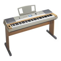