13
TNY274-280
E
2/06
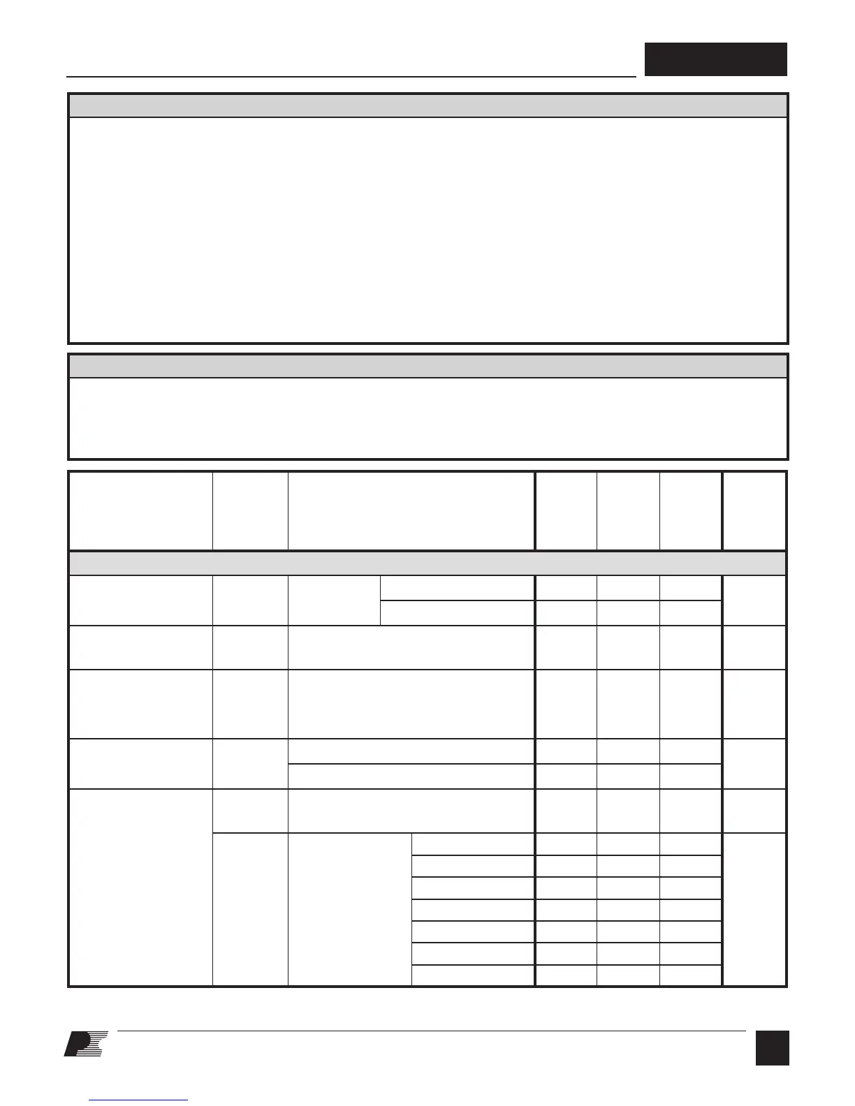
Parameter Symbol
Conditions
SOURCE = 0 V; T
J
= -40 to 125 °C
See Figure 16
(Unless Otherwise Specified)
Min Typ Max Units
CONTROL FUNCTIONS
Output Frequency
in Standard Mode
f
OSC
T
J
= 25 °C
See Figure 4
Average 124 132 140
kHz
Peak-Peak Jitter 8
Maximum Duty
Cycle
DC
MAX
S1 Open 62 65 %
EN/UV Pin Upper
Turnoff Threshold
Current
I
DIS
-150 -115 -90 µA
EN/UV Pin
Voltage
V
EN
I
EN/UV
= 25 µA 1.8 2.2 2.6
V
I
EN/UV
= -25 µA 0.8 1.2 1.6
DRAIN Supply
Current
I
S1
EN/UV Current > I
DIS
(MOSFET Not
Switching) See Note A
290 µA
I
S2
EN/UV Open
(MOSFET
Switching at f
OSC
)
See Note B
TNY274 275 360
µA
TNY275 295 400
TNY276 310 430
TNY277 365 460
TNY278 445 540
TNY279 510 640
TNY280 630 760
ABSOLUTE MAXIMUM RATINGS
(1,5)
DRAIN Voltage .................................. ..............-0.3 V to 700 V
DRAIN Peak Current: TNY274.......................400 (750) mA
(2)
TNY275.....................560 (1050) mA
(2)
TNY276.....................720 (1350) mA
(2)
TNY277.....................880 (1650) mA
(2)
TNY278...................1040 (1950) mA
(2)
TNY279 ................. 1200 (2250) mA
(2)
TNY280 ................. 1360 (2550) mA
(2)
EN/UV Voltage ................................................... -0.3 V to 9 V
EN/UV Current ........................................................... 100 mA
BP/M Voltage .................................................. ....-0.3 V to 9 V
Storage Temperature ......................................-65 °C to 150 °C
Operating Junction Temperature
(3)
.................-40 °C to 150 °C
Lead Temperature
(4)
....................................................... 260 °C
Notes:
1. All voltages referenced to SOURCE, T
A
= 25 °C.
2. The higher peak DRAIN current is allowed while the
DRAIN voltage is simultaneously less than 400 V.
3. Normally limited by internal circuitry.
4. 1/16 in. from case for 5 seconds.
5. Maximum ratings specified may be applied one at a time,
without causing permanent damage to the product.
Exposure to Absolute Maximum Rating conditions for
extended periods of time may affect product reliability.
THERMAL IMPEDANCE
Thermal Impedance: P or G Package:
(θ
JA
) ........................... 70 °C/W
(2)
; 60 °C/W
(3)
(θ
JC
)
(1)
............................................... 11 °C/W
Notes:
1. Measured on the SOURCE pin close to plastic interface.
2. Soldered to 0.36 sq. in. (232 mm
2
), 2 oz. (610 g/m
2
) copper clad.
3. Soldered to 1 sq. in. (645 mm
2
), 2 oz. (610 g/m
2
) copper clad.
 Loading...