PROJECT
TITLE
Radom.XIANG
CHECKED BY
Mountain.ZHOU
DRAWN BY
OF
A
6
5
4
32
1
SHEET
A
B
C
D
123456
D
C
B
Quectel Wireless Solutions
SIZE
VER
83
1.0
DATE
2015/3/30
EC20 Reference Design
A2
e.g. 5V
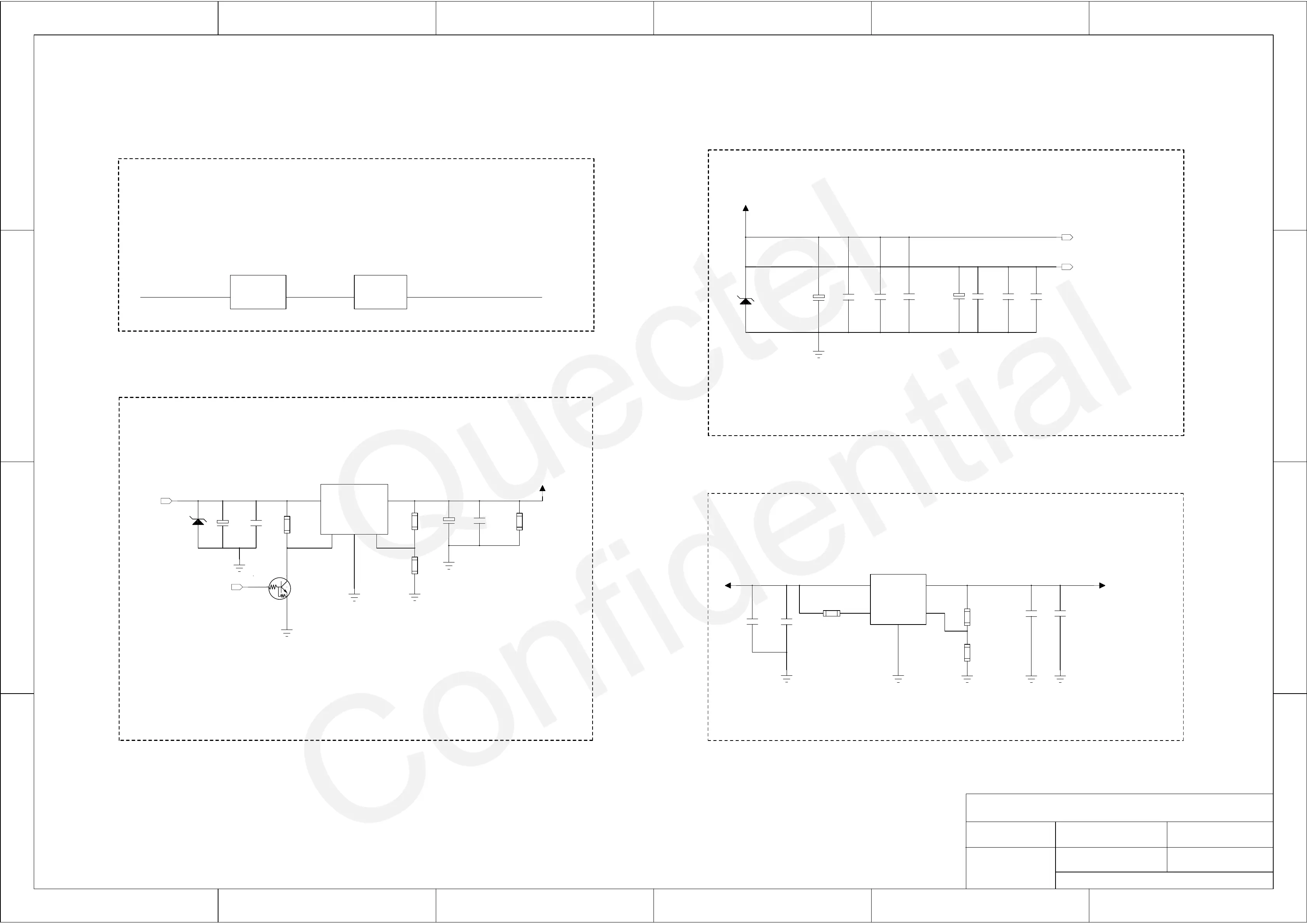
LDO Application
It is used when the input voltage is below 7V.
VBAT = (R302/R303+1)*1.24 = 3.88V
DC-DC Application
It is used when the input voltage is above 7V. Use DC-DC to convert high input
e.g. DC12V IN
DC-DC
DC 5V out
LDO
DC 3.8V out for module
voltage to 5V, and LDO will generate 3.8V typical voltage for the module.
VDD_3.0V = (R305/R306+1)*1.207 = 3.0V
Supply Power for PCM Codec and SD Card
Close to the module VBAT pins
Note:
VBAT should be routed in star mode to VBAT_BB and VBAT_RF pins.
Power Supply Design
VBAT Design
Connect to VBAT_BB pins
Connect to VBAT_RF pins
Power Design
+
C303
470uF
1
EN
2
IN
3
GND
4
OUT
5
ADJ
U301
MIC29302WU
C304
100nF
C302
100nF
+
C301
470uF
R302
100K
1%
R303
47K
1%
1
IN
3
EN
5
OUT
4
BP
2
GND
U302
SGM2019-ADJ
C316
4.7uF
R305
63.4K
1%
R306
42.2K
1%
C317
100nF
R304
51K
C314
1uF
C315
100nF
+
C305
100uF
D301
PZ3D4V2H
R301
51K
C306
100nF
C307
33pF
C308
10pF
C310
100nF
C311
33pF
C312
10pF
+
C309
100uF
R307
470R
D302
TVS
Q301
DTC043ZEBTL
DC_IN
VBAT
VDD_3.0V
VBAT
[1,3,8]
VBAT
[1,3,8]
VBAT
VBAT
[2]
VBAT_EN