1
1
2
2
3
3
4
4
5
5
6
6
D D
C C
B B
A A
7
200 Scenic View Dr.
Cumberland, RI 02864 78/4/2020
Sheet: of
NK49-Power.SchDoc
NK49-MAIN.PrjPcb
Originally Drawn By:
Project:
Sheet:
Variant: Production
Last Modified By:
Last Modified:
Copyright 2019, inMusic Brands
All Rights Reserved
Rev I
D36
MBRA340T3G
TP27
TP26
1
2
3 4
5
6
D33
USBLC6-2
0.1uF
50V
C265
1.00MR346
0.1uF
50V
C266
USB-A
GND
USB1_D1_N
USB1_D1_P
L6
90ohms@100MHz
VBUS
1
D-
2
D+
3
GND
4
56
SHLD
J20
TYPE-B-2.0
USB1_D2_N
USB1_D2_P
1
2
3 4
5
6
D34
USBLC6-2
0.1uF
50V
C274
1.00MR348
0.1uF
50V
C275
USB-B
GND
USB2_D1_N
USB2_D1_P
L8
90ohms@100MHz
VBUS
1
D-
2
D+
3
GND
4
56
SHLD
J22
TYPE-B-2.0
USB2_D2_N
USB2_D2_P
L4
0.0nH
L7
0.0nH
+8V0
-8V0
VERTICAL
1
2
J30
SIL UNSHROUDED 3.96mm
VERTICAL
1
2
J29
SIL UNSHROUDED 3.96mm
+28-C
GND
+28-B
GND
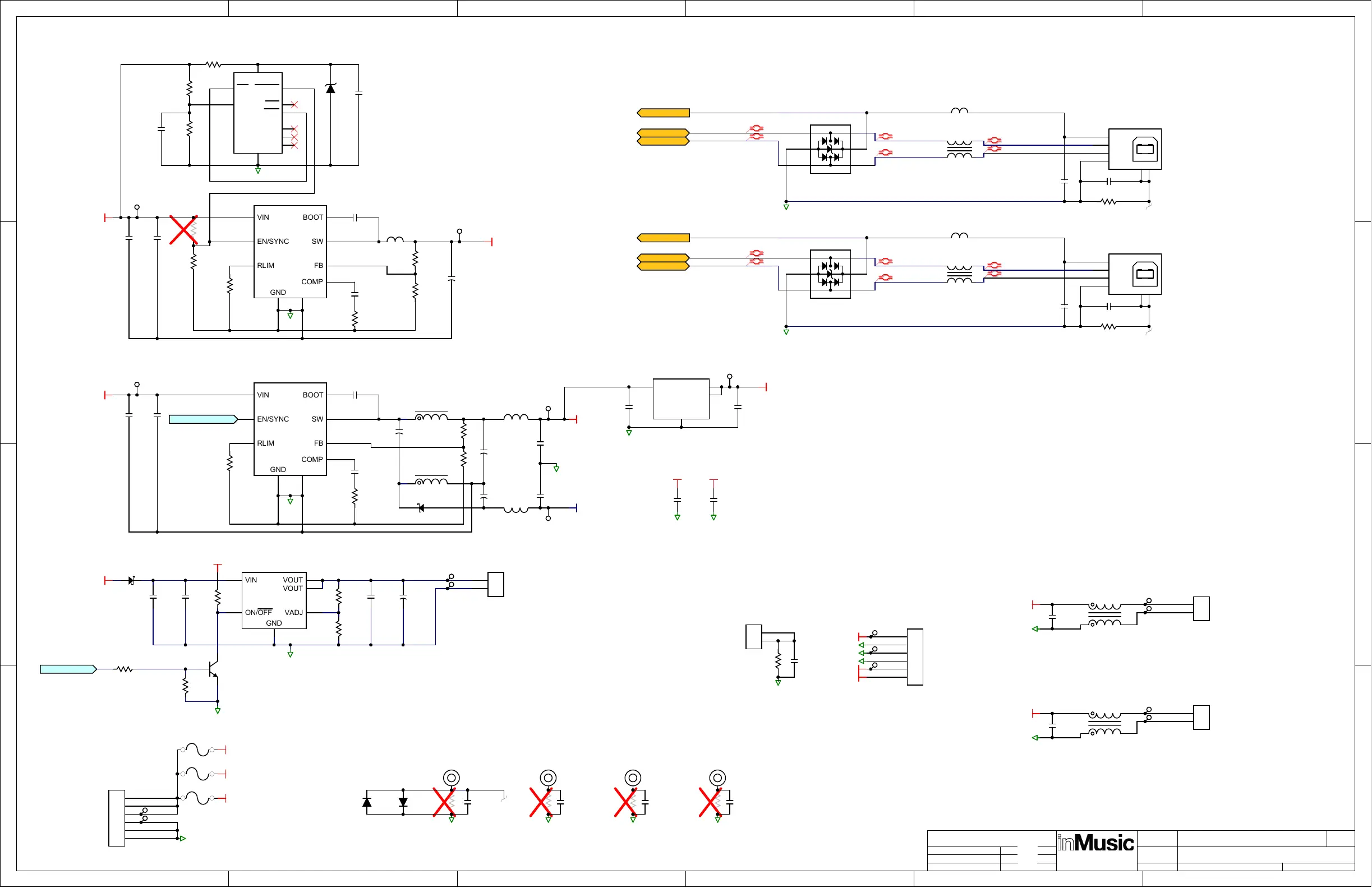
90 ohms differential impedance between
USB_D_N & USB_D_P on PCB and cable.
GND
GND
GND
F2
1.6A 250V
F3
1A 250V
F1
1.6A 250V
+28-A
+28-B
+28-C
From
Universal AC
Mains
To Center Board
+3V3
1
2
3
4
5
6
VERTICAL
J31
SIL SHROUDED 2.0mm
0.1uF
50V
C294
0.00
R369
0.1uF
50V
C295
0.00
R370
GND
+3V3
PMIC_ON_REQ5
USB1_D_N5
USB1_D_P5
USB2_D_N5
USB2_D_P5
USB1_VBUS5
USB2_VBUS5
USB1_D_N
USB1_D_P
USB2_D_N
USB2_D_P
3 4
1 2
L13
130uH
3 4
1 2
L14
130uH
22uF
35V
C300
22uF
35V
C301
ESD
ESD
ESD
Star Ground to J32-3/4
+28-A
TP24
TP23
COMP
6
VIN
8
SW
1
GND
4
BOOT
2
EN/SYNC
3
RLIM
7
FB
5
GND
9
U38 RT7272B
L9
22uH
22uF
35V
C168
56.2K
R263
8.06K
R269
23.7K
R289
10.5K
R267
2,200pF
50V
C182
0.1uF
50V
C167
GND
0.1uF
50V
C170
3.32K
R271
1 3
L15A
47uH
2 4
L15B
47uH
+28-A
TP25
COMP
6
VIN
8
SW
1
GND
4
BOOT
2
EN/SYNC
3
RLIM
7
FB
5
GND
9
U40 RT7272B
22uF
35V
C208
23.7K
R294
2,200pF
50V
C267
0.1uF
50V
C207
GND
0.1uF
50V
C261
20.0K
R290
2.21K
R291
0.1uF
50V
C264
0.1uF
50V
C269
GND
L12
10uH
L16
10uH
45.3K
R270
45.3K
R293
33uF
10V
+
C171
33uF
10V
+
C263
33uF
10V
+
C268
33uF
10V
+
C262
+3V3
+28-A
D55
MBRS140T3
22uF
35V
C270
0.1uF
50V
C271
10.0K
R268
220uF
35V
+
C273
0.1uF
50V
C272
39.2K
R295
2.21K
R297
VIN
1
ON/OFF
2
VOUT
3
VADJ
4
GND
5
VOUT
6
U25 NJM2387
GND
3
1
2
Q39
2222A
10.0K
R299
GND
FAN_PWM5
1.26V
1
2
VERTICAL
J33
SIL SHROUDED 2.0mm
24V-FAN Fan: 24 V; 33 mA; 40x40x20 mm
Sunon MF40202V2-10000-A99
3.32KR298
+5V0
GND
Vin
3
VOUT
2
4
GND
1
U37 1117S50
10uF
10V
C161
TP22
0.1uF
50V
C159
+5V0
GND
+3V3
MTG2 MTG3 MTG4MTG1
GND
0.1uF
50V
C209
22uF
35V
C211
22uF
35V
C212
+3V3
GND
+3V3
GND
0.1uF
50V
C165
0.00
R232
GNDGND
0.00
R233
1
2
J18
GROUND LUG
GND
0.00
R341
0.1uF
50V
C210
1
2
3
4
5
6
J32
SIL UNSHROUDED 3.96mm
TP31
TP32
TP49
TP58
TP60
TP59
TP61
TP62
TP63
TP64
TP65
CHANGE LOG:
1) Reduced post DAC gain by 1.4 dB to match DAC
R168, R183, R63, R162, R188, R197
2) Adjusted SPI termination at J13 to improve signal quality and reduce EMI.
Replaced the following with RC network:
L29,L28,L27, L17, L18, L19, L20, L21, L22, L23
3) Removed FET switch for 3V3SW. Supplies will come up together to avoid boot failure.
Delete the following: R368, D37, Q34, R366, Q32
Change +3V3SW to +3V3
4) Reduced C162 codec reset cap to 100pf (was delaying muting)
5) Added test points to JTAG header
6) Fixed audio output mute
7) Add caps to 3 signals on both J11 and J12
8) Removed left and right PLT0/1
9) Added RST to +3.3V buck enable to prevent fast power cycle erro
D37
MURS160
D35
MURS160
MTG1, MTG2, MTG3, MG4 must connect to Earth GND via stand offs to bottom chassis
Chassis bottom must be Earth grounded
NOTE:
Do not stuff R232, R233, R369, R370
100K
R288
0.1uF
50V
C317
5.76K
R292
3.16K
R236
1uF
16V
C316
Vth=1.25V
Delays +3.3V Buck turn-on 200ms
Allows +3.3V to fully discharge before restart
GND
Enables buck at 2.5V
R263 not fitted
D56
5.1V
MR
2
PFI
3
NC
4
PFO
8
LLO
7
NC
6
RESET
10
NC
9
GND
5
VCC
1
U42
LM3704
 Loading...