RTL8773E Motherboard User Guide
9
·Copyright 2019 Realtek Semiconductor Corporation.
All Rights Reserved.
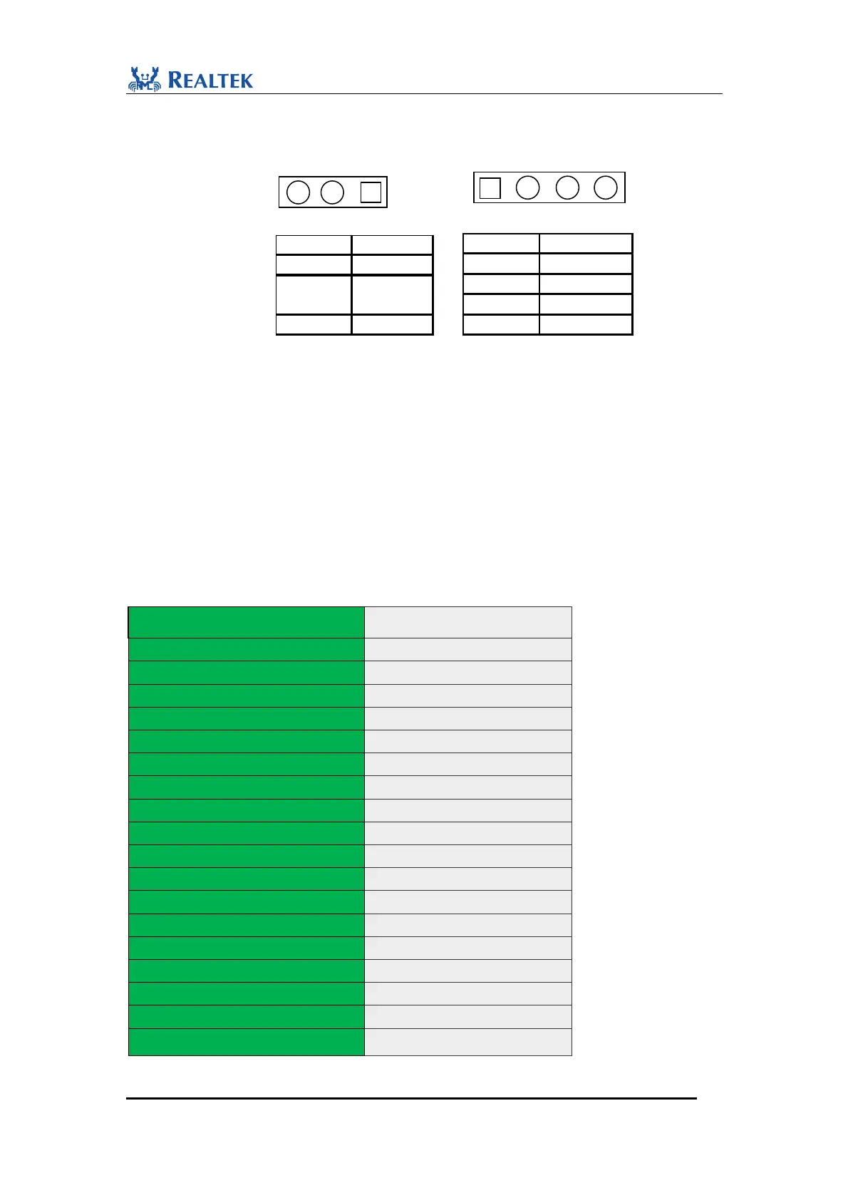
Pin Description
1 VDDIO1
2 FT_VDDIO
3 VDD102
1 2 3
J33
1 2 3
Pin Description
1 MICBIAS
2 MIC4_N
3 MIC4_P
4 GND
4
J20
1.4 IO Pins Assignment
The RTL8773E Motherboard is designed to fit RTL8773E EVB daughter board. All
common interfaces installed on evaluation board are available to each IO pin of
RTL8773E chip by connecting control jumpers to different RTL8773E chip’s IOs.
The default pin assignment is performed by directly shorting pins of RTL8773E
Motherboard and common interfaces on control jumper.
For example, J3 is used for LEDs’ and KEY s’ control. Short Pin1 and Pin2 on control
jumper, LED1 is controlled by M0_1 of RTL8773E Motherboard
Table 1-1 Default Pin Assignment for Common Interfaces on RTL8773E Motherboard
EVB Daughter board Mother board socket name
M0_0/ADC_0 M0_0/THM_DET
M0_1/ADC_1 M0_1/LED1&KEY1
M0_2/ADC_2 M0_2
M0_3/ADC_3 M0_3
M0_4/ADC_4 M0_4
M0_5/ADC_5 M0_5
M0_6/ADC_6 M0_6
M0_7/ADC_7 M0_7
M1_0 M1_0/LED2&KEY2
M1_1 M1_1/KEY0
M1_2 M1_2/KEY1
M1_3 M1_3/LED4
M1_4 M1_4/KEY2
M1_5 M1_5/KEY3
M1_6 M1_6/JTAG_TDO
M1_7 M1_7
M2_0 M2_0
M2_1 M2_1/LED3&KEY3
 Loading...