Ameba-ZII Application Note
Application Note All information provided in this document is subject to legal disclaimers. © REALTEK 2018. All rights reserved.
7
List of Figures
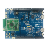
Figure 1-1 Top View of Ameba-ZII 2V0 Dev Board ............................................................................................ 9
Figure 1-2 Ameba-ZII 2V0 Dev Board PCB Layout .............................................................................................. 9
Figure 1-3 Pin Out Reference for DEV_2V0 ..................................................................................................... 11
Figure 3-1 Connection between J-Link Adapterand Ameba-ZII SWD connector ............................................. 12
Figure 3-4 Log UART via FT232 on EVB V2.0 .................................................................................................... 14
Figure 4-1 AmebaZII Image Tool UI .................................................................................................................. 22
Figure 4-2 Ameba-ZII EVB V2.0 Hardware Setup ............................................................................................. 23
 Loading...