Renesas RA Microcontrollers EK-RA4M1 v1 – User's Manual
R20UT4579EU0100 Rev.1.00 Page 16 of 32
Oct.02.19
Table 4. J-Link Interface Conflicts
SSLB0 fixed function, J1-13
MOSIB fixed function, J1-7
GTIOC0A fixed function, J1-31
5.4.3 JTAG/SWD
A 10-pin Cortex
®
Debug Connector is provided at J10.
Table 5. JTAG/SWD Connector (J10)
N.C. (short E31 to connect to GND)
The Cortex
®
Debug Connector is fully described in the Arm
®
CoreSight
™
Architecture Specification.
The J-Link MCU Power copper jumper and J-Link Disconnects copper jumpers may be
open for proper operation of the JTAG interface to prevent interactions with the J-Link
MCU. See section 5.4.2, Debug USB for details.
If a JTAG adapter is in use that properly interprets the Arm
®
Cortex
®
10-pin Debug
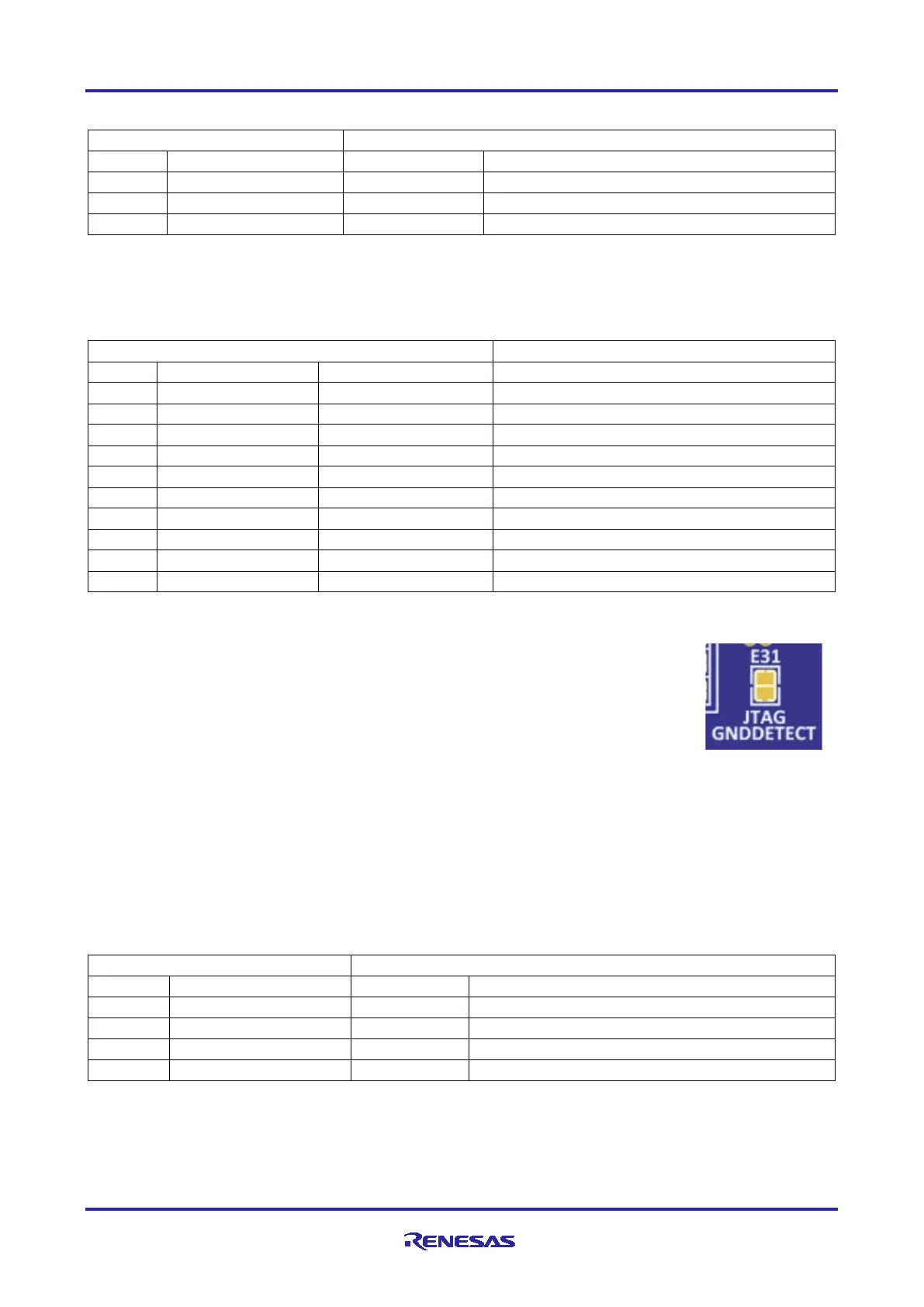
Connector assignment of pin 9 to GND, the JTAG GNDDetect copper jumper E31
should be closed. If the JTAG adapter used is one of several that may be confused or
damaged by the presence of GND at pin 9, E31 should be open (as shipped).
The J-Link
®
OB interface is multiplexed with the JTAG interface, and can collectively be referred to as the
Programming Interface. While the J-Link
®
OB interface and the JTAG interface do not conflict, the J-Link
®
OB signals may be isolated from the programming interface by changing the copper jumpers as described in
section 5.4.2, Debug USB.
Four of the JTAG ports (P108, P109, P110, and P300) are multiplexed with the SPI Fixed Pin function on pin
header of J1. To use these signals for the SPI function, the J-Link debug function must be disabled. Details
of the multiplexed signals are shown in the following table.
Table 6. JTAG Interface Conflicts
SSLB0_B fixed function, J1-13
MOSIB_B fixed function, J1-7
MISOB_B fixed function, J1-9
GTIOC0A_A fixed function, J1-31

 Loading...


