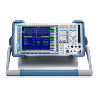
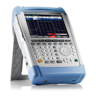
R&S FSH Instrument Design and Functional Description
1145.5973.82 3.1 E-11
3 Repair
T
his chapter describes the design of the R&S FSH, simple measures for repair and troubleshooting,
and, in particular, the replacement of modules.
Firmware updates and the installation of the DTF option are described in Chapter 4.
Instrument Design and Functional Description
The following figure shows a block diagram of the R&S FSH.
4 - 7 GHz
I
N
1
00 kHz ..
6 GHz
P
rotection
Attenuator
LowPass
Filter
IF 1a
Mixer Filter
IF 2a
Mixer Filter
IF 3
Mixer Buffer
To
Mainboard
3
.2 GHz
800 MHz
0 - 3
GHz
4
031
MHz
8
31.25
MHz
3
1.25
MHz
4 - 7
GHz
3
.2
GHz
: 4
Oscillator 1
(LO 1)
Oscillator 2
(LO 2)
Synthesizer
Noise
12
ADC
10
M
Hz
TCXO
3615.6
or 4031.2
MHz
Mixer
TG OUT
REF
Reference
Oscillator
(TG)
12
12
Audio
OUT
Power
Adapter
18 V
Battery
+
Temp
Sense
Key pad
LCD
Module
EEPROM
Inter-
connection
Board
Trigger
Power
Sensor
Power and
Battery
Management
Risc
Controller
Data
Memory
Program
Memory
DATA Detector
Address, DATA and Control Bus
Audio and TRIGGER
Optical
Interface
Optical
Adapter
Mainboard
Filter
IF 1b
Mixer Filter
IF 2b
Mixer
7231
MHz
3
- 6
GHz
x2
5.1 - 6.6 GHz
x2
3.2 GHz
xN
N = 1 for f < 3 GHz
N = 2 for f > 3 GHz
FSH6 only
Fig. 3-1 Block Diagram R&S FSH
 Loading...

