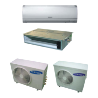
6-12 Samsung Electronics
6-2. OUTDOOR PCB Diagram
RJ040F2HXEA/RJ050F2HXEA MAIN PCB
1
2
3
4
5
6
7
8
91011 12 1314
15
16
1 CN701-EEV A 2 CN851-Snet 3 CN252-OLP Sensor 4 CN951 Main -SUB
#1~#4 : Motor signal # Not use #1~#2 : OLP Sensor #1 5V
#5 : DC 12V #2~#5 Sensor
#6~#9 EEV B signal
#11~#14 Grid1~4
#15~#21 Segmanet7~1
#22~#25 Kin4~1
#27 Gnd
#28 12V
5 CN030-4WAY 6 TB-L 7 TB-N 8 EARTH
#1~#3 : 220~240 Vac #AC Power(220V) : L #AC Power(220V) : N #Earth
9 CN251 - Sensor 10 CN201-MICOM DOWN 11 CN952-Central-CTL 12 CN910-BLDC FAN
#1~#2 Out-TH #1~#10 MICOM DOWN
#not use
#1 : DC 360V
#3~#4 Dis-TH (main micom) #2 : N.C
#5~#6 Cond-TH #3 : GND
#4 : DC 15V
#5 : FAN RPM
#6 : FAN RPM feedback
13 CN13-MICOM DOWN 14 CN451-COMP 15 Cn051-REACTOR 16 CN301-COMM
#1~#10 MICOM DOWN #1 W phase #1~#2 : REACTOR #1 : COM1
(inverter micom)
#2 V phase #2 : COM2
 Loading...