Reference Information
2-2 Samsung Electronics
2. Camera power
Camera power block consists of IC120 (PWM IC MB3800), Q121 (INVERTER TR DTC144EU), Q122 (SWITCH-
ING TR KSD1621), and rectifier circuit.
When CAM5V control pin of LCD MICOM 10PIN is high, it is converted at Q121 and IC 120. Pin 4 becomes low;
then IC120 Pin 7 starts oscillating and the PWM output from IC120 Pin 5 switches Q122. Pin 6 generates the 15V
output by a switching pulse and this output is rectified by D121, L123, C127, and C128 to generate 15V power for
the drive of CCD (IC201) and V DRIVE IC (MN3112SA).
The pulse for -7V (which is generated at T121 pin 10), is rectified by D121, C129, L124, C130 and becomes -7V
power for the drive of CCD and V DRIVE IC.
The pulse for 5V power, which is output from T121 pin 7, becomes CAMERA 5V power by D122, C133, L127, and
C134. The 5V power is divided by D5V for the drive of IC204(MN5246) and IC202(MN3112SA) and A5V for the
drive of IC203, IC205, and IC206 through L125.
3. SYS 5V
Using the same technique as with camera 5V (L141, IC140, Q142, and T141), the SYS 5V power drives IC301,
IC302, IC303, IC304 and IC307, and is generated by SYS 5V CONT from the LCD micom.
EVER5V power is always output when battery and adapter are connected; SYS 5V power is output only when
power is turned on. CAM power is output for 0.5 second (only during shot operation).
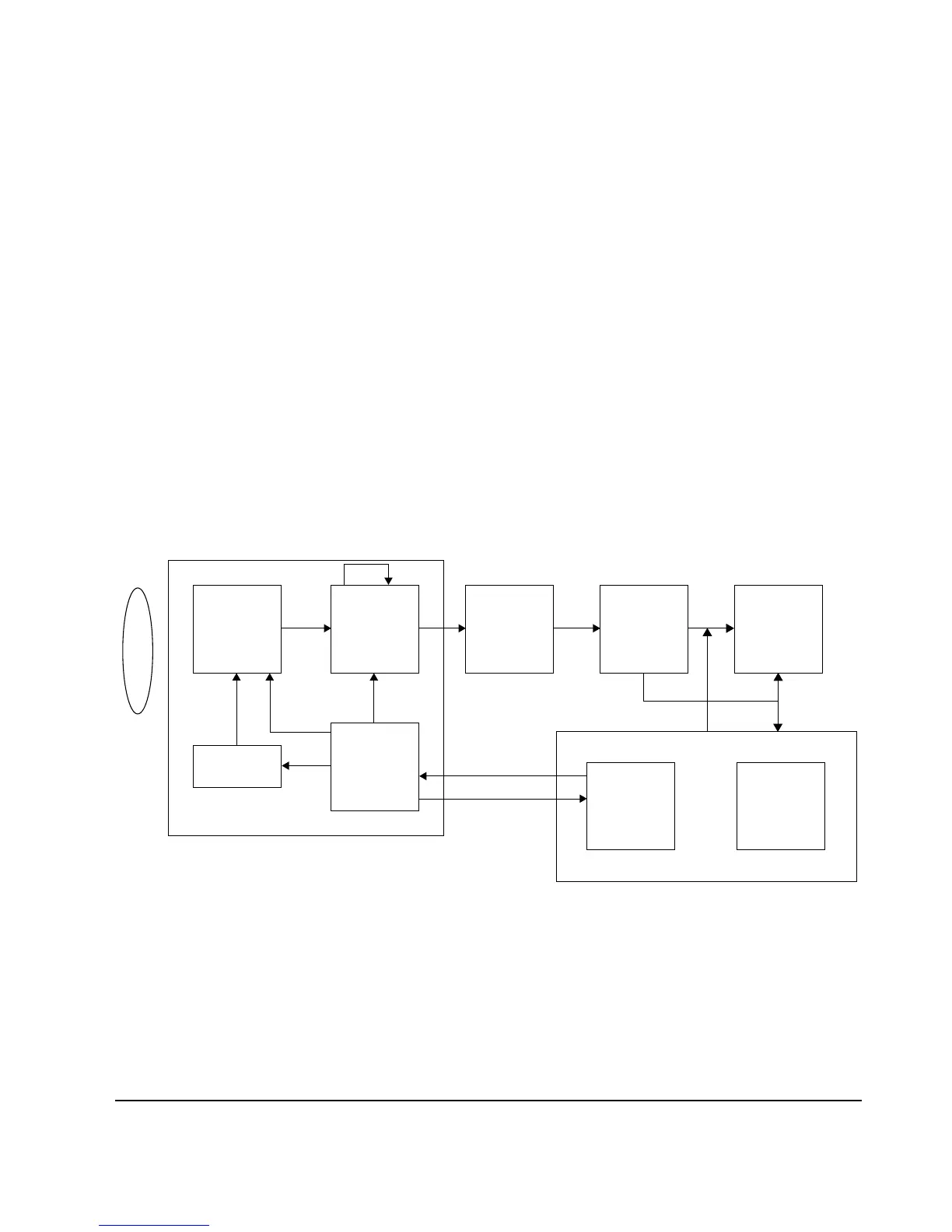
2-1-4 Camera
1. Camera operation
Fig. 2-1
The image from the lens is converted to an electrical signal by the photoelectric conversion component, CCD
(MN3776PE). Each pulse used to extract CCD signal is generated by the timing geneartor IC(MN5246),
converted to actual driving voltage by V Drive IC(MN3112SA), and supplied to CCD. After noise elimination
(CDS) and amplification (AGC) at analog process IC(NN2038FAQ), CCD output signal is converted to a digital
signal by A/D converter. The 8-bit digital data is changed to 16-bit by DRAM control IC(SMA9606), and stored in
the DRAM.
CCD
1/3" 35
Vout Vout
CDS out
AGC IN
D7~D0
Data 8
D15~D0
Data 16
16
Address
A9~A1
D Data, DCLK
HD, VD
SMD
SHP
R
H1
H2
V1~V4
VSUB
RISC Chip
CDS
AGC
V-Drive
LENS
Timing
Gen
A/D
(8bit)
8-16 CONV.
DRAM CTRL
DRAM
4Mb
Camera
Ctrl
S/W
DSCP
 Loading...