CS4955 PIN ASSIGNMENTS
PIN NAME NUMBER TYPE DEFINITION
V[7:0] 8,7,6,5,4,3,2,1 IN Digital video data inputs
CLK 29 IN 27MHz input clock
PADR 16 IN Address enable line
XTAL-IN 15 IN Sub-carrier crystal input
XTAL-OUT 14 OUT Sub-carrier crystal output
HSYNC/CB 10 I/O Active low horizontal sync, or composite blank s ignal
VSYNC 11 I/O Active low vertical sync
FIELD/CB 9 OUT Video field ID. Selectable polarity or composite blank
RD 27 IN Host parallel port read strobe, active low
WR 28 IN Host parallel port write strobe, active low
PDAT[7:0] 19,20,21,22,23,24,25,26 I/O Host parallel port/general purpose I/O
SDA 32 I/O I C data
SCL 33 IN I C clock input
CVBS 44 CURRENT Composite video output
Y 48 CURRENT Luminance analog output
C 47 CURRENT Chrominance analog output
R 39 CURRENT Red analog output
G 40 CURRENT Green analog output
B 43 CURRENT Blue analog output
VREF 38 I/O Internal voltage reference output external reference input
SET 37 CURRENT DAC current set
TTXDAT 30 IN Teletext data input
TTXRQ 31 OUT Teletext request output
INT 12 OUT Interrupt output, active high
RESET 34 IN Active low master RESET
TEST 13 IN Test pin. Ground for normal operation
VAA 36,41,46 PS +5V or +3.3Vsupply(must be same as VDD)
GNDD 18 PS Ground
VDD 17 PS +5V or +3.3Vsupply(must be same as VAA)
GNDA 35,42,45 PS Ground
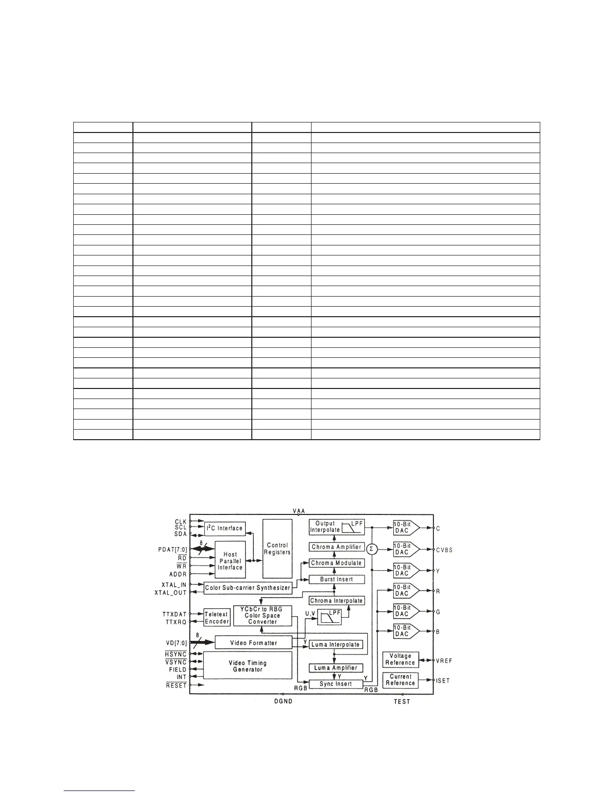
CS4955 BLOCK DIAGRAM
17
 Loading...