PCM1723 PIN ASSIGNMENTS
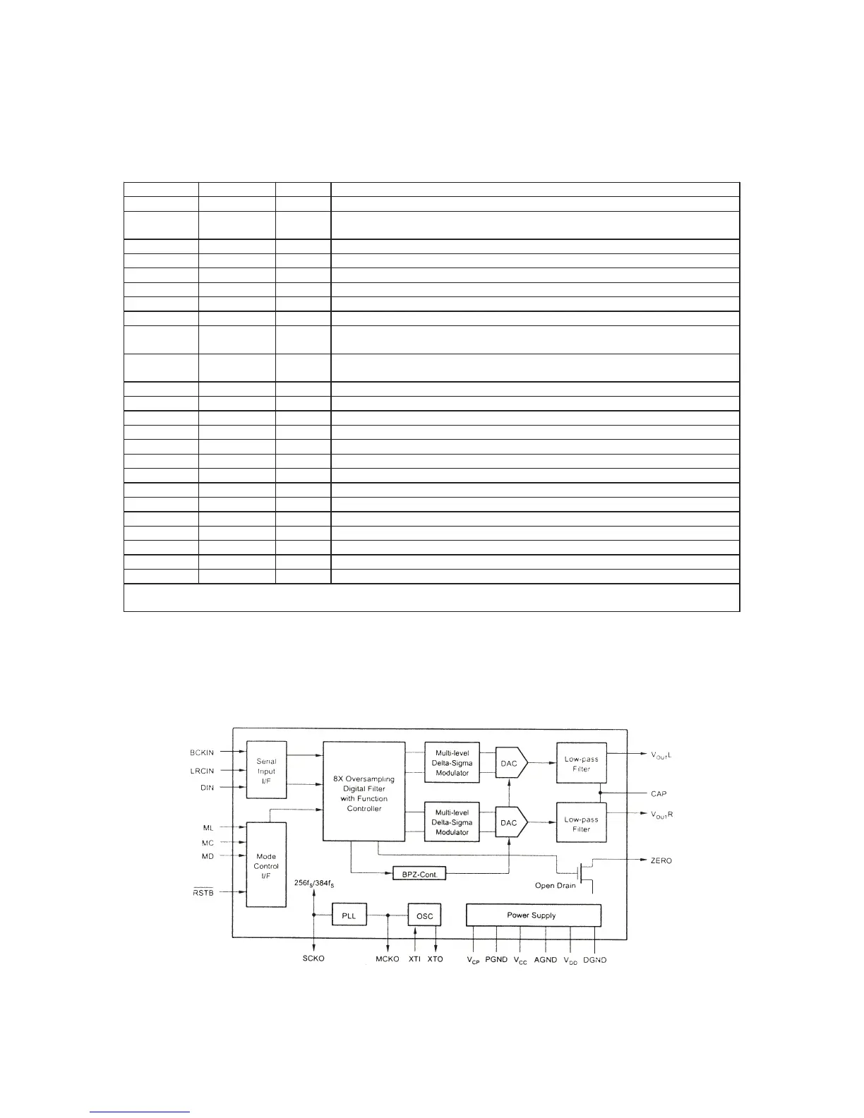
PCM1723 BLOCK DIAGRAM
PIN NAME NUMBER TYPE DEFINITION
XTI 1 IN Master clock input
SCKO 2 OUT
System Clock Out. This output is 256fs or 384fs.System clock generated
by the internal PLL.
VCP 3 PWR PLL Power Supply (+5v)
NC 4 N/A No connection
MCKO 5 OUT Buffered clock output of crystal oscillator
ML 6 IN Latch for serial control data
MC 7 IN Clock for serial control data
MD 8 IN Data for serial control
RSTB 9 IN
Reset input. When this pin is low, the digital filters and modulator are held
in reset
ZERO 10 OUT
Zero Data Flag. This pin is low when the input data is continuously zero for
more than 65.535 cycles of BCKIN
VOUTR 11 OUT Right Channel Analog Output
AGND 12 GND Analog Ground
VCC 13 PWR Analog Power Supply(+5v)
VOUTL 14 OUT Left Channel Analog Output
CAP 15 Common pin for analog output amplifiers
BCKIN 16 IN Bit clock for clocking in the audio data
DIN 17 IN Serial audio data input
LRCIN 18 IN Left/Right Word Clock. Frequency is equal to fs
NC 19 N/A No connection
RES 20 N/A Reserved for factory use, do not connect
VDD 21 PWR Analog Power Supply(+5v)
DGND 22 GND Digital Ground
PGND 23 GND PLL Ground
XTO 24 OUT Crystal oscillator output
Note:(1)Schmitt triger input with internal pull-up res istors.
(2)Schmitt triger input.
18
 Loading...