NR 1 ØnD3 17
key 4
30 KEQ NL XC3 1 2 XC2
2 ØnD7 31 KMC § XC4 3 4 XC1
3 ØnD1 18
key 5
32 KMR § ØnD16 5 6 T
4 ØnD5 19
key 6
33 KMS § ØnD13 7 8 ØnB8
5
K
20
key 7
34 KMAS § ØnD12 9 10 Ø3
6 ØnD4 21
key 8
35 PMANUAL ØnD11 11 12 Ø2
7 Ø1 22
key 9
36 — — 13 14 Ø1
8 nPXI 23 KCLR 37 — ØnD1 15 16 ØnD1
9
key RC
24 KMD 38 IDLE ØB1 17 18 —
10 VDD 25 KCE 39 Ø3 ØB2 19 20 —
11
K
26 KD 40 P ØB4 21 22 —
12 ØB1 27 PTRIGGER 41 — ØB8 23 24 —
13
key 0
28 KDP 42 GND — 25 26 —
14
key 1
43 nDPØD GND 27 28 GND
15
key 2
29 KS 44 X VCL 29 30 VCL
16
key 3
45 — VDD 31 32 VDD
— 33 34 —
nPXI 35 36 —
— 37 38 ØnD4
— 39 40 ØnD3
— 41 42 ØnD5
— 43 44 ØnD7
NK ØnD3 1 2 ØnD7
ØnD1 3 4 ØnD5
K
5 6 ØnD4
Ø1 7 8 nPXI
KRC 9 10 VDD
K
11 12 ØB1
key 0
13 14
key 1
key 2
15 16
key 3
key 4
17 18
key 5
key 6
19 20
key 7
key 8
21 22
key 9
KCLR 23 24 KMD
KCE 25 26 KD
PTRIGGER 27 28 KDP
KS 29 30 KEQ
§ KMC 31 32 KMR §
§ KMS 33 34 KMAS §
PMANUAL 35 36
lamp *
lamp ÷
37 38 IDLE
Ø3 39 40 P
—
41 42 GND
nDPØD 43 44 X
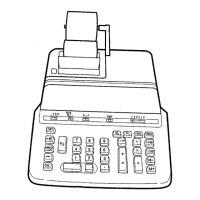
Sharp Compet 17 Calculator
Section: IC Pinouts and Gate Construction
Page: 16 Rendition: 2020 May 20
Dual 8-bit Shift Register
Discrete Gate Construction
Most OR and some AND gates are constructed from discrete diodes and
resistors. More complex logic elements are contained in integrated circuits. The
internal construction of discrete gates is shown in the following diagrams. A
wire–OR or wire–AND construction is indicated by the input line traversing the
width of the gate.
AND Gate OR Gate OR Gate
with ‘wired’ input
The diodes and resistors may be individual components or contained in
TDA001 and TDA002 packages.
Most gate outputs have load resistors (
R
) connected from the output to one
side of the power supply. To reduce clutter these resistors are indicated in the
schematic by one of the following letters (
r
) in a box near the output.
Symbol (
r
) Resistance (
R
)
A 15K to VDD
B 20K to VDD
C 30K to VDD
D 50K to VDD
E 100K to VDD
H 150K to VDD
J 300K to VDD
K 300K to VCL
nn
470K to VCL, internal to TDA002 unit
nn
a 40K to GND
b 60K to GND
c 100K to GND
d 300K to GND
Occasionally individual MOSFET transistors or MOSFETs contained in µPD7
ICs are used as AND gates. The gate of these transistors functions as an
inverted input. Because the MOSFET is a bidirectional device, a diode is usually
required on the other input or the output to prevent ‘backflow’ of the signal.
Special mention must be made of the unusual use of a µPD7 for the 4-bit
display latch. Controlling pin 6 allows it to function as a sample-and-hold latch,
presumably relying on inter-electrode capacitance to hold the state between
digit updates (see Display).
The µPD Integrated Circuit Family
♦ Based on supply voltage, circuit impedances and logic density, IC technology is presumed to be early MOS.
♦ Gate symbols are presented in accordance with:
logic 1 = 0V, GND
logic 0 = –24V
♦ Outputs are open-collector, closing to GND (logic 1) and requiring external pull-down resistor to –24V (logic 0).
♦ Inferred for flip-flops:
The flip-flops in this logic family appear to be Master/Slave D-type flip-flops with the clocks for the master and slave sections
kept separate. This permits a system design where data capture is done in accordance with the requirements of the logic while all
outputs are changed synchronously by a single clock signal.
ØC = Capture Input (master section clock)
ØT = Transition Input (slave section clock)
The state of the D input is captured when ØC is logic 0 (–24V).
The Q output is set in accordance with the captured state when ØT goes to logic 0.
 Loading...