LC-37D90U
5 – 27
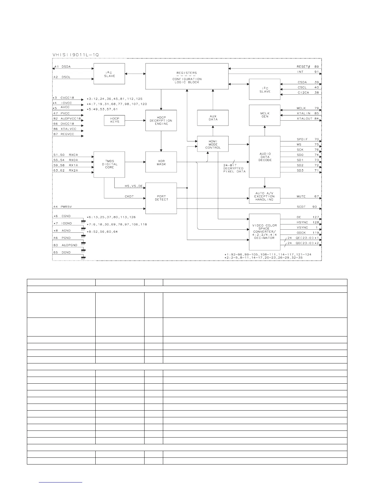
2.7. VHiSii9011L-1Q (ASSY: IC1508)
HDMI/DVI Receiver
• Block Diagram [VHiSii9011L-1Q (ASSY: IC1508)]
• Pin Function [VHiSii9011L-1Q (ASSY: IC1508)]
Pin No. Pin Name I/O Pin Function
Digital Video Output Pins
92, 93, 94, 95, 96, 99, 100,
101, 102, 103, 104, 105, 108,
109, 110, 111, 114, 115, 116,
117, 121, 122, 123, 124
QE23-0 O 24-Bit Even Pixel.
2, 3, 4, 5, 8, 9, 10, 11, 14, 15,
16, 17, 20, 21, 22, 23, 26, 27,
28, 29, 32, 33, 34, 35
QO23-0 O 24-Bit Odd Pixel.
127 DE O Data enable.
128 HSYNC O Horizontal Sync.
1 VSYNC O Vertical Sync.
119 ODCK O Output Data Clock.
Digital Audio Output Pins
85 XTALIN I Crystal Clock Input.
84 XTALOUT O Crystal Clock Output.
79 MCLK I/O Audio Master Clock Input Reference.
76 SCK O I2S Serial Clock Output.
75 WS O I2S Word Select Output.
74 SD0 O I2S Serial Data Output.
73 SD1 O I2S Serial Data Output.
72 SD2 O I2S Serial Data Output.
71 SD3 O I2S Serial Data Output.
70 SPDIF O S/PDIF Audio Output.
67 MUTE O Mute Audio Output.
Configuration/Programming Pins
91 INT O Interrupt Output.
89 RESET# I Reset Pin. Active LOW.