LC-37D90U
5 – 57
2.16. VHiTC6384AF1EQ (ASSY: IC8702)
SD_CARD_CONTROLER
• Pin Function [VHiTC6384AF1EQ (ASSY: IC8702)]
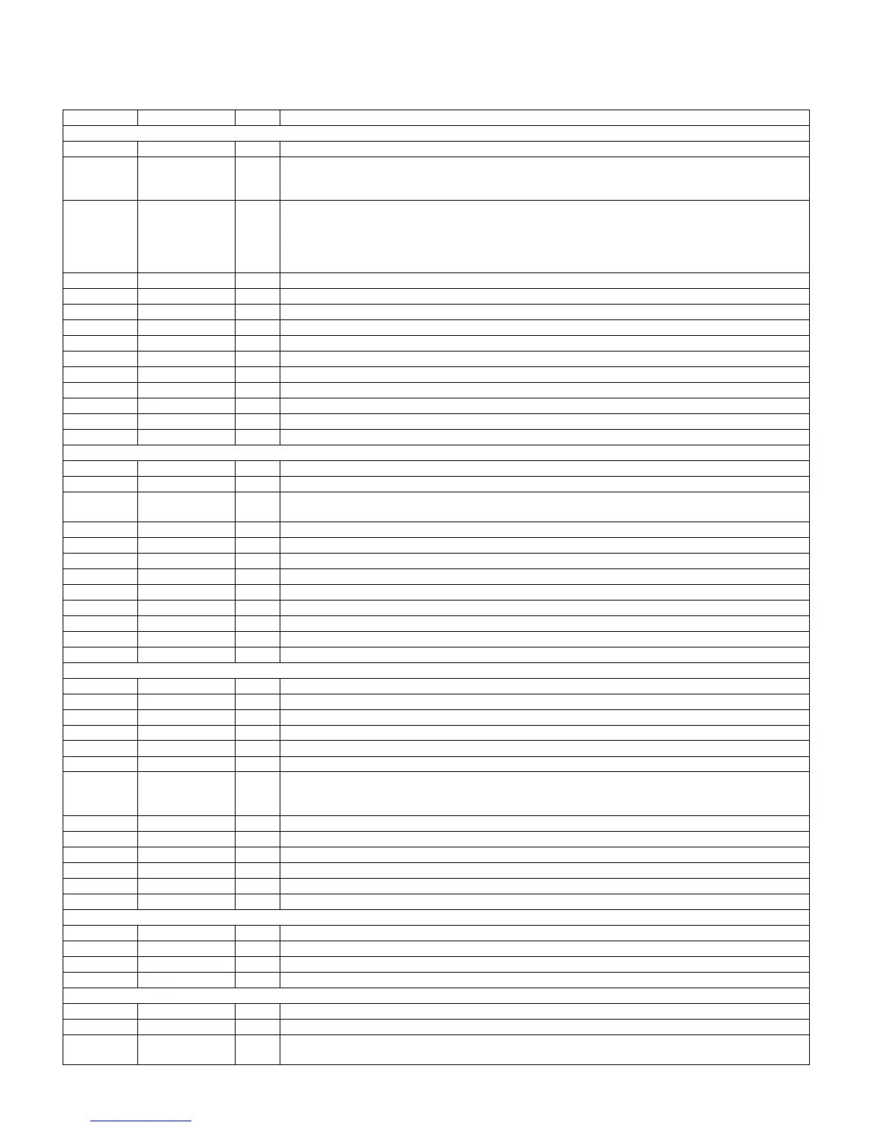
Pin No. Pin Name I/O Pin Function
Host interface
76 #CS I Chip select (accessible in #CS= “0”).
98, 97, 94,
93, 88, 85,
82, 77
A [7:0] I Address bit 7-0.
13, 11, 10,
8, 4, 2, 1,
99, 95, 89,
83, 81, 75,
74, 70, 68
D [15:1] I/O Data bit [15:0].
67 #RE I Read enable. The content of the register is output to D [15:0] when making it to “0”.
100 #WE I Write enable. When “0” is connected by three clocks, D [15:0] value is written in the register.
7 BE1 I Byte enable. Most Significant Byte becomes accessible at BE1=BEPOL.
12 BE0 I Byte enable. Least Significant Byte becomes accessible at BE0=BEPOL.
66 BEPOL I Polarity setting of BE [1:0].
86 #ACK O Acnorigge signal when register is accessed.
87 #RQ O Interrupt output.
62 ASYNC I Change of method in host interface.
79 MCLK I Main clock.
6 MCLK2 I SD card detection clock.
91 #RESET I Main reset.
SD CARD interface
50 SDCLK O SD clock. Slot 1 and 2 using combinedly.
38 SD1CMD I/O SD command output. Response input (slot 1).
36, 37, 42,
45
SD1DAT [3:0] I/O SD data. Bit [3:0] (Slot1).
47 #SD1CD I SD detection input (Slot1).
41 SD1WP I SD write-protection input (Slot1).
39 SD2CMD I/O SD command output. Response input (slot 2). #FWPSD and sharing.
22 SD2DAT3 I/O SD data. Bit3 (Slot2).
24 SD2DAT2 I/O SD data. Bit2 (Slot2). #FRE and sharing.
30 SD2DAT1 I/O SD data. Bit1 (Slot2). #FWE and sharing.
34 SD2DAT0 I/O SD data. Bit0 (Slot2). #FCE and sharing.
27 #CD2 I SD detection input.
16 SD2WP I SD write-protection input (Slot2).
Smart Media interface
25 #SMUSE I When Smart Media is used for slot 2, it is assumed, “0”.
34 #FCE O Smart Media chip enable. SD2DAT0 and sharing.
35 FCLE O Smart Media command latch enable.
23 FALE O Smart Media address latch enable.
24 #FRE O Smart Media Read enable. SD2DAT0 and sharing.
30 #FWE O Smart Media Write enable. SD2DAT1 and sharing.
17, 18, 20,
21, 31, 32,
44, 46
FD [7:0] I/O Smart Media data. Bit [7:0].
29 #FBSY I Smart Media Ready/busy input signal.
14 #FWP O Smart Media write-protection output signal.
49 #EJECTIN I Smart Media eject demand signal.
56 #EJECTOUT O Smart Media eject response signal.
27 (#CD2) I Smart Media card detection signal (SD2 and using combinedly).
39 #FWPSD I Smart Media write-protection seal detection signal (SD2CMD and using combinedly).
DSP interface
57 ACCLK O A-CORE clock output (“0” fixed output).
55 #ACREQ I A-CORE request input (Please input “0” or “1” and stabilize potential).
52 ACDATA O A-CORE data output (“0” fixed output).
54 ACVALID O A-CORE effective horsepower (“0” fixed output).
Other
73 DIP1 I DIP input terminal for debugging.
72 DIP0 I DIP input terminal for debugging.
71 LED3 O LED output terminal for debugging. It synchronizes with the LED bit of the SM_MCR register though it is
controlled by an internal register.
 Loading...