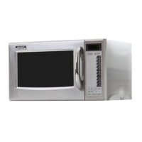
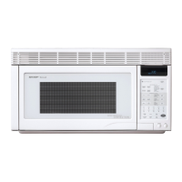
R-15AT
19
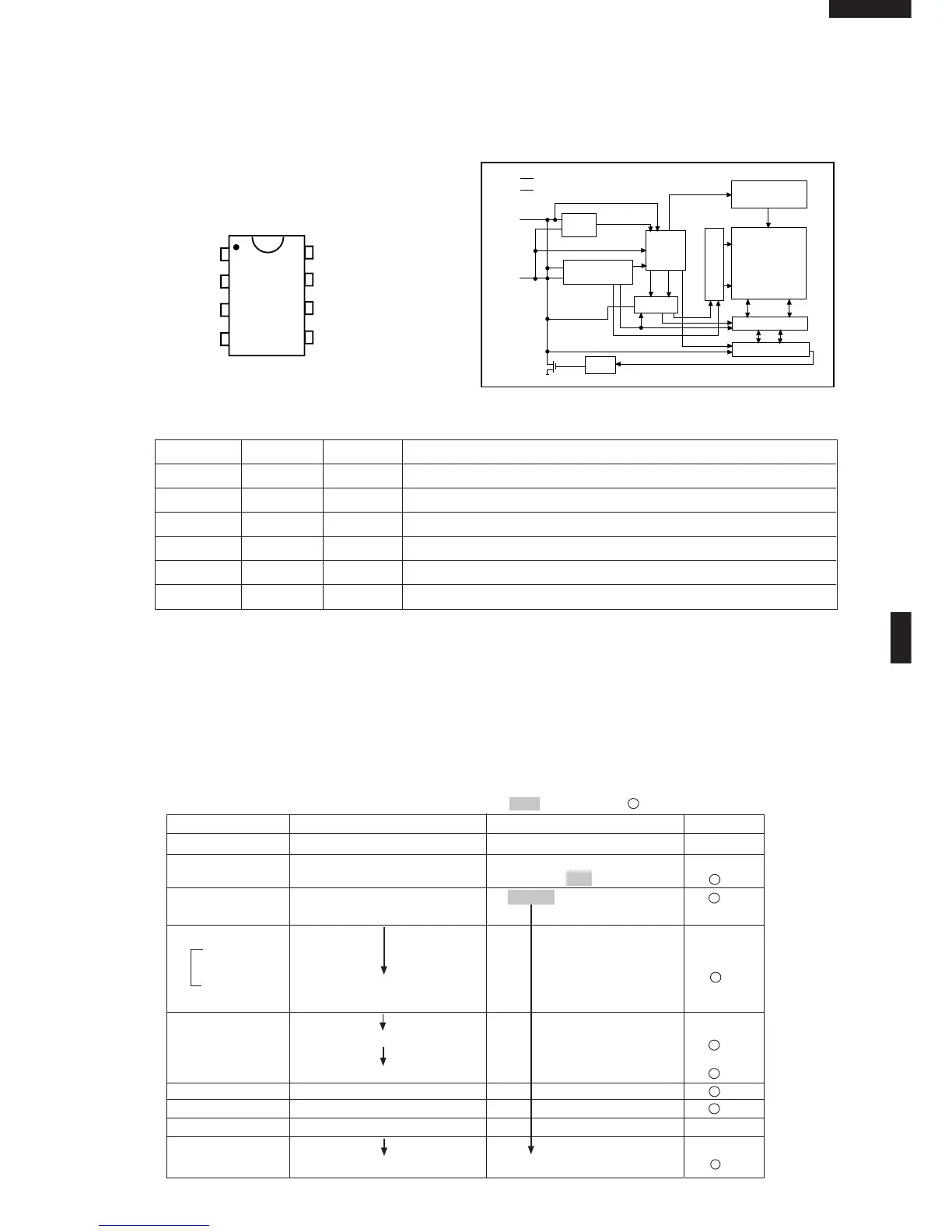
AT24C02 is a 2K-bit, serial memory, enabling CMOS to be erased/written electrically. This memory is constructed with
256 registers x 8bits, enabling individual access, read and write operations to be performed. Details of input/output signal
for IC2 are as shown in the following diagram.
2-2 Memory IC (IC2)
Table 1. Relation between Pin Nos, and Signals
Pin No. Signal I/O Description
1-3 A0-A2 IN Connected to +5V.
4 VSS IN Connected to GND.
5 SDA IN/OUT Serial data input/output : input/outputs data to IC1.
6 SCL IN Clock signal input : input/outputs sireal data at every one pulse.
7 TEST IN Connected to GND.
8 VCC IN Connected to +5V.
1
A1
A2
VSS
VCC
TEST
SCL
SDA
TOP VIEW
A0
2
3
4
8
7
6
5
When the memory IC (IC2) or control unit is exchanged, input the relay timing to the memory IC (IC2), referring to the
“how to input the relay timing”. Otherwise the oven will make a big noise when starting.
How to input the relay timing
... Flashing / ... 0.1sec BUZZER
PAD DISPLAY INDICATOR PHONE
(Door close) .
.
CHECK . CHECK No.
CHECK 82 68 CHECK
(user total count)
SIGNAL
SIGNAL
DOUBLE 34 56
QUANTITY (service total count upper figure 3456XX)
7 7 No.
(after 1 sec.) 38 69
SET 0
3,8,4,9 38 49 x 4
SET 38 49
CHECK .