20
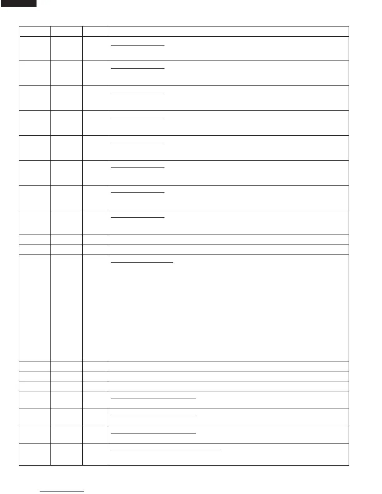
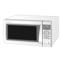
R-308DW
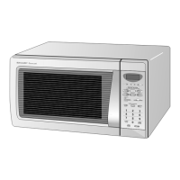
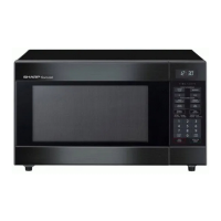
R-310DK
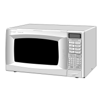
R-310DW
33 P27 OUT Key strobe signal.
Signal applied to touch-key section. A pulse signal is input to P41, P43, P44 and P45
terminal while one of G8 line keys on key matrix is touched.
34 P26 OUT Key strobe signal.
Signal applied to touch-key section. A pulse signal is input to P41, P43, P44 and P45
terminal while one of G7 line keys on key matrix is touched.
35 P25 OUT Key strobe signal.
Signal applied to touch-key section. A pulse signal is input to P41, P43, P44 and P45
terminal while one of G6 line keys on key matrix is touched.
36 P24 OUT Key strobe signal.
Signal applied to touch-key section. A pulse signal is input to P41, P43, P44 and P45
terminal while one of G5 line keys on key matrix is touched.
37 P23 OUT Key strobe signal.
Signal applied to touch-key section. A pulse signal is input to P41, P43, P44 and P45
terminal while one of G4 line keys on key matrix is touched.
38 P22 OUT Key strobe signal.
Signal applied to touch-key section. A pulse signal is input to P41, P43, P44 and P45
terminal while one of G3 line keys on key matrix is touched.
39 P21 OUT Key strobe signal.
Signal applied to touch-key section. A pulse signal is input to P41, P43, P44 and P45
terminal while one of G2 line keys on key matrix is touched.
40 P20 OUT Key strobe signal.
Signal applied to touch-key section. A pulse signal is input to AN0, P41, P43, P44 and
P45 terminal while one of G1 line keys on key matrix is touched.
41-48 P17-P10 OUT Terminal not used.
49-50 P07-P06 OUT Terminal not used.
51-72
SEG21-SEG0
OUT Segment data signal.
Connected to LCD.
The relation between signals are as follows:
LSI signal (Pin No.) LCD (Pin No.) LSI signal (Pin No.) LCD (Pin No.)
SEG 21 (51) .................................. SEG3 SEG 10 (62) ...............................SEG14
SEG 20 (52) .................................. SEG2 SEG 9 (63) ...............................SEG13
SEG 19 (53) .................................. SEG1 SEG 8 (64) ...............................SEG12
SEG 18 (54) ................................ SEG22 SEG 7 (65) ...............................SEG11
SEG 17 (55) ................................ SEG21 SEG 6 (66) ...............................SEG10
SEG 16 (56) ................................ SEG20 SEG 5 (67) .................................SEG9
SEG 15 (57) ................................ SEG19 SEG 4 (68) .................................SEG8
SEG 14 (58) ................................ SEG18 SEG 3 (69) .................................SEG7
SEG 13 (59) ................................ SEG17 SEG 2 (70) .................................SEG6
SEG 12 (60) ................................ SEG16 SEG 1 (71) .................................SEG5
SEG 11 (61) ................................ SEG15 SEG 0 (72) .................................SEG4
73/74 VCC/VREF IN Connected to GND.
75 AVSS IN Connected to VC.
76 COM3 OUT Terminal not used.
77 COM2 OUT Common data signal: COM1.
Connected to LCD signal C1.
78 COM1 OUT Common data signal: COM2.
Connected to LCD signal C2.
79 COM0 OUT Common data signal: COM3.
Connected to LCD signal C3.
80 VL3 IN Power source voltage input terminal.
Standard voltage for LCD.
Pin No. Signal I/O Description