R-4A54
R-4A54B
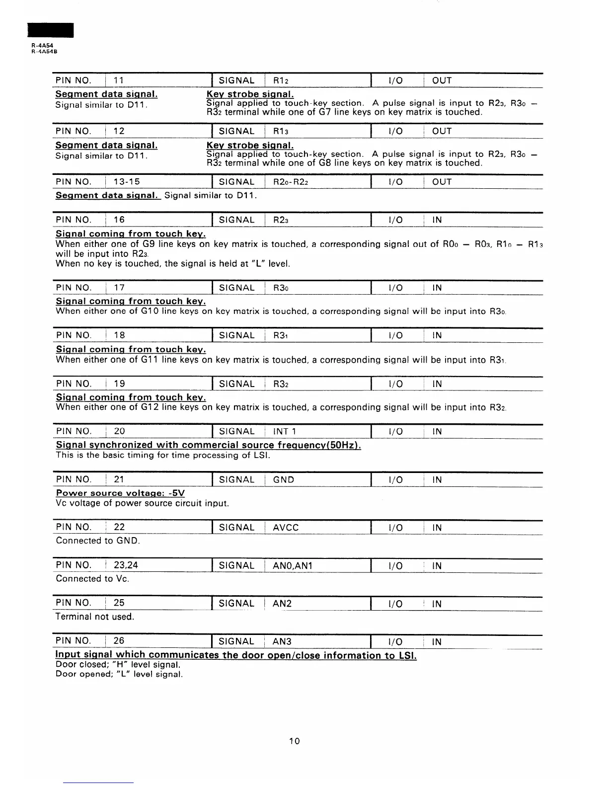
/ 11 PIN NO.
Seoment data signal.
Signal similar to Dl 1.
f SIGNAL /
R12
I
l/O
i OUT
Key strobe signal.
Signal applied to touch-key section. A pulse signal is input to R23, R3o -
R32 terminal while one of G7 line keys on key matrix is touched.
PIN NO.
! 12
Seament data signal.
Signal similar to Dll.
1 SIGNAL j RI3
I
I/O
i OUT
Kev strobe signal.
Signal applied to touch-key section. A pulse signal is input to R23, R3o -
R32 terminal while one of G8 line keys on key matrix is touched.
PIN NO. i 13-15
1 SIGNAL / R2o-R22
I i/o
/ OUT
Segment data signal. Signal similar to Dll.
PIN NO. i 16
1 SIGNAL 1 R23 1 l/O / IN
Signal cominn from touch kev.
When either one of G9 line keys on key matrix is touched, a corresponding signal out of ROo - RO3, RIO - RI3
will be input into R23.
When no key is touched, the signal is held at “L” level.
PIN NO. ; 17
1 SIGNAL j R30
I
I/O
/ IN
Signal comino from touch kev.
When either one of GIO line keys on key matrix is touched, a corresponding signal will be input into R3o.
PIN NO. 1 18
1 SIGNAL i R37
I
I/O
/ IN
Signal coming from touch kev.
When either one of Gll line keys on key matrix is touched, a corresponding signal will be input into R31.
PIN NO. I 19
SIGNAL / R32
I
i/O
I IN
Signal coming from touch kev.
When either one of G12 line keys on key matrix is touched, a corresponding signal will be input into R32.
PIN NO. i 20
I SIGNAL i INT 1
I
I/O
1 IN
Signal svnchronized with commercial source freouencv(50Hz).
This is the basic timing for time processing of LSI.
PIN NO. i 21
1 SIGNAL / GND
Power source voltaoe: -5V
VC voltage of power source circuit input.
I
l/O
i IN
PIN NO. ; 22
Connected to GND.
1 SIGNAL / AVCC
I
I/O
i IN
PIN NO.
! 23,24
Connected to VC.
1 SIGNAL / ANO,ANl
I
I/O
; IN
PIN NO.
j 25
1 SIGNAL 1 AN2
I I/O
: IN
Terminal not used.
PIN NO.
j 26
1 SIGNAL ; AN3
I
i/O
: IN
Input signal which communicates the door open/close information to LSI.
Door closed; “H” level signal.
Door opened; “L” level signal.
IO
 Loading...